- 您现在的位置:买卖IC网 > PDF目录4057 > MPC8360ECVVAJDGA (Freescale Semiconductor)IC MPU POWERQUICC II PRO 740TBGA PDF资料下载
参数资料
| 型号: | MPC8360ECVVAJDGA |
| 厂商: | Freescale Semiconductor |
| 文件页数: | 14/102页 |
| 文件大小: | 0K |
| 描述: | IC MPU POWERQUICC II PRO 740TBGA |
| 标准包装: | 21 |
| 系列: | MPC83xx |
| 处理器类型: | 32-位 MPC83xx PowerQUICC II Pro |
| 速度: | 533MHz |
| 电压: | 1.2V |
| 安装类型: | 表面贴装 |
| 封装/外壳: | 740-LBGA |
| 供应商设备封装: | 740-TBGA(37.5x37.5) |
| 包装: | 托盘 |
| 配用: | MPC8360EA-MDS-PB-ND - KIT APPLICATION DEV 8360 SYSTEM MPC8360E-RDK-ND - BOARD REFERENCE DESIGN FOR MPC |
第1页第2页第3页第4页第5页第6页第7页第8页第9页第10页第11页第12页第13页当前第14页第15页第16页第17页第18页第19页第20页第21页第22页第23页第24页第25页第26页第27页第28页第29页第30页第31页第32页第33页第34页第35页第36页第37页第38页第39页第40页第41页第42页第43页第44页第45页第46页第47页第48页第49页第50页第51页第52页第53页第54页第55页第56页第57页第58页第59页第60页第61页第62页第63页第64页第65页第66页第67页第68页第69页第70页第71页第72页第73页第74页第75页第76页第77页第78页第79页第80页第81页第82页第83页第84页第85页第86页第87页第88页第89页第90页第91页第92页第93页第94页第95页第96页第97页第98页第99页第100页第101页第102页
MPC8360E/MPC8358E PowerQUICC II Pro Processor Revision 2.x TBGA Silicon Hardware Specifications, Rev. 5
Freescale Semiconductor
19
DDR and DDR2 SDRAM DC Electrical Characteristics
6.1
DDR and DDR2 SDRAM DC Electrical Characteristics
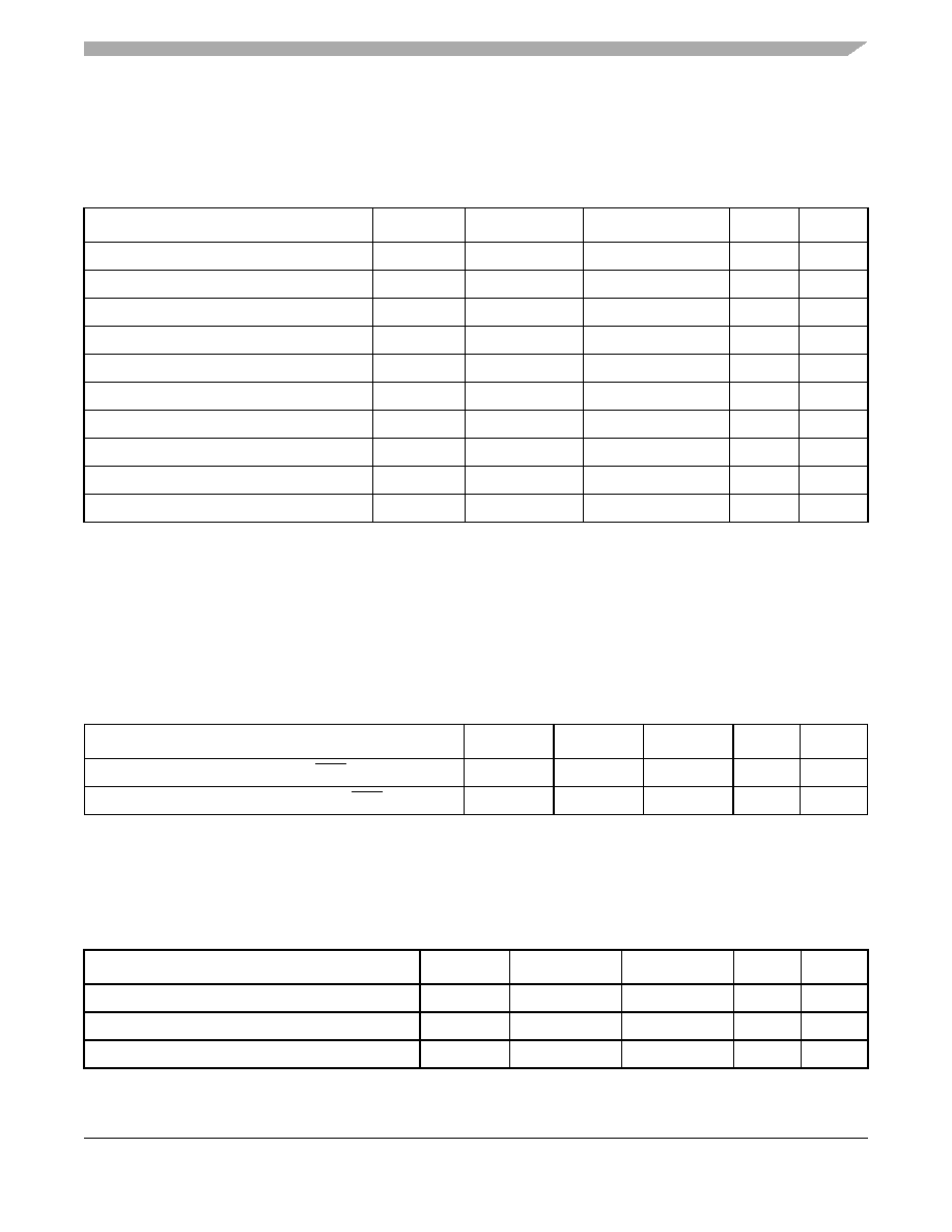
This table provides the recommended operating conditions for the DDR2 SDRAM component(s) of the device when
GVDD(typ) = 1.8 V.
This table provides the DDR2 capacitance when GVDD(typ) = 1.8 V.
This table provides the recommended operating conditions for the DDR SDRAM component(s) of the device when
GVDD(typ) = 2.5 V.
Table 14. DDR2 SDRAM DC Electrical Characteristics for GVDD(typ) = 1.8 V
Parameter/Condition
Symbol
Min
Max
Unit
Notes
I/O supply voltage
GVDD
1.71
1.89
V
1
I/O reference voltage
MVREF
0.49
× GVDD
0.51
× GVDD
V
2
I/O termination voltage
VTT
MVREF – 0.04
MVREF + 0.04
V
3
Input high voltage
VIH
MVREF + 0.125
GVDD + 0.3
V
—
Input low voltage
VIL
–0.3
MVREF – 0.125
V
—
Output leakage current
IOZ
—±10
μA
4
Output high current (VOUT = 1.420 V)
IOH
–13.4
—
mA
—
Output low current (VOUT = 0.280 V)
IOL
13.4
—
mA
—
MVREF input leakage current
IVREF
—±10
μA—
Input current (0 V
≤VIN ≤OVDD)IIN
—±10
μA—
Notes:
1. GVDD is expected to be within 50 mV of the DRAM GVDD at all times.
2. MVREF is expected to equal 0.5 × GVDD, and to track GVDD DC variations as measured at the receiver. Peak-to-peak noise
on MVREF cannot exceed ±2% of the DC value.
3. VTT is not applied directly to the device. It is the supply to which far end signal termination is made and is expected to equal
MVREF. This rail should track variations in the DC level of MVREF.
4. Output leakage is measured with all outputs disabled, 0 V
≤V
OUT ≤GVDD.
Table 15. DDR2 SDRAM Capacitance for GVDD(typ)=1.8 V
Parameter/Condition
Symbol
Min
Max
Unit
Notes
Input/output capacitance: DQ, DQS, DQS
CIO
68
pF
1
Delta input/output capacitance: DQ, DQS, DQS
CDIO
—0.5
pF
1
Note:
1. This parameter is sampled. GVDD = 1.8 V ± 0.090 V, f = 1 MHz, TA = 25°C, VOUT = GVDD/2, VOUT (peak-to-peak) = 0.2 V.
Table 16. DDR SDRAM DC Electrical Characteristics for GVDD(typ) = 2.5 V
Parameter/Condition
Symbol
Min
Max
Unit
Notes
I/O supply voltage
GVDD
2.375
2.625
V
I/O reference voltage
MVREF
0.49
× GVDD
0.51
× GVDD
V
I/O termination voltage
VTT
MVREF – 0.04
MVREF + 0.04
V
相关PDF资料 |
PDF描述 |
|---|---|
| XF2B-1745-31A | CONN FPC 17POS 0.3MM PITCH SMD |
| FMM43DSEN-S243 | CONN EDGECARD 86POS .156 EYELET |
| XCS20-3PQ208C | IC FPGA 5V C-TEMP 208-PQFP |
| XCS10XL-5VQ100C | IC FPGA 3.3V C-TEMP 100-VQFP |
| XCS10XL-5TQ144C | IC FPGA 3.3V C-TEMP 144-TQFP |
相关代理商/技术参数 |
参数描述 |
|---|---|
| MPC8360ECVVAJDHA | 制造商:FREESCALE 制造商全称:Freescale Semiconductor, Inc 功能描述:PowerQUICC II Pro Processor Revision 2.x TBGA Silicon Hardware Specifications |
| MPC8360ECVVAJFGA | 制造商:FREESCALE 制造商全称:Freescale Semiconductor, Inc 功能描述:PowerQUICC II Pro Processor Revision 2.x TBGA Silicon Hardware Specifications |
| MPC8360ECVVAJFHA | 制造商:FREESCALE 制造商全称:Freescale Semiconductor, Inc 功能描述:PowerQUICC II Pro Processor Revision 2.x TBGA Silicon Hardware Specifications |
| MPC8360ECVVALDGA | 制造商:FREESCALE 制造商全称:Freescale Semiconductor, Inc 功能描述:PowerQUICC II Pro Processor Revision 2.x TBGA Silicon Hardware Specifications |
| MPC8360ECVVALDHA | 制造商:FREESCALE 制造商全称:Freescale Semiconductor, Inc 功能描述:PowerQUICC II Pro Processor Revision 2.x TBGA Silicon Hardware Specifications |
发布紧急采购,3分钟左右您将得到回复。