- 您现在的位置:买卖IC网 > PDF目录4065 > MPC8377VRALGA (Freescale Semiconductor)MPU POWERQUICC II 667MHZ 689PBGA PDF资料下载
参数资料
| 型号: | MPC8377VRALGA |
| 厂商: | Freescale Semiconductor |
| 文件页数: | 92/127页 |
| 文件大小: | 0K |
| 描述: | MPU POWERQUICC II 667MHZ 689PBGA |
| 标准包装: | 27 |
| 系列: | MPC83xx |
| 处理器类型: | 32-位 MPC83xx PowerQUICC II Pro |
| 速度: | 667MHz |
| 电压: | 1V |
| 安装类型: | 表面贴装 |
| 封装/外壳: | 689-BBGA 裸露焊盘 |
| 供应商设备封装: | 689-TEPBGA II(31x31) |
| 包装: | 托盘 |
第1页第2页第3页第4页第5页第6页第7页第8页第9页第10页第11页第12页第13页第14页第15页第16页第17页第18页第19页第20页第21页第22页第23页第24页第25页第26页第27页第28页第29页第30页第31页第32页第33页第34页第35页第36页第37页第38页第39页第40页第41页第42页第43页第44页第45页第46页第47页第48页第49页第50页第51页第52页第53页第54页第55页第56页第57页第58页第59页第60页第61页第62页第63页第64页第65页第66页第67页第68页第69页第70页第71页第72页第73页第74页第75页第76页第77页第78页第79页第80页第81页第82页第83页第84页第85页第86页第87页第88页第89页第90页第91页当前第92页第93页第94页第95页第96页第97页第98页第99页第100页第101页第102页第103页第104页第105页第106页第107页第108页第109页第110页第111页第112页第113页第114页第115页第116页第117页第118页第119页第120页第121页第122页第123页第124页第125页第126页第127页
MPC8377E PowerQUICC II Pro Processor Hardware Specifications, Rev. 8
Freescale Semiconductor
67
15.5
Receiver Compliance Eye Diagrams
The Rx eye diagram in Figure 43 is specified using the passive compliance/test measurement load (see
Figure 44) in place of any real PCI Express Rx component. In general, the minimum receiver eye diagram
measured with the compliance/test measurement load (see Figure 44) is larger than the minimum receiver
eye diagram measured over a range of systems at the input receiver of any real PCI Express component.
The degraded eye diagram at the input receiver is due to traces internal to the package as well as silicon
parasitic characteristics that cause the real PCI Express component to vary in impedance from the
Unexpected Electrical Idle
Enter Detect Threshold
Integration Time
An unexpected electrical idle
(Vrx-diffp-p <
Vrx-idle-det-diffp-p) must be
recognized no longer than
Trx-idle-det-diff-entertime to
signal an unexpected idle
condition.
TRX-IDLE-DET-DIFF-
ENTERTIME
——
10
ms
—
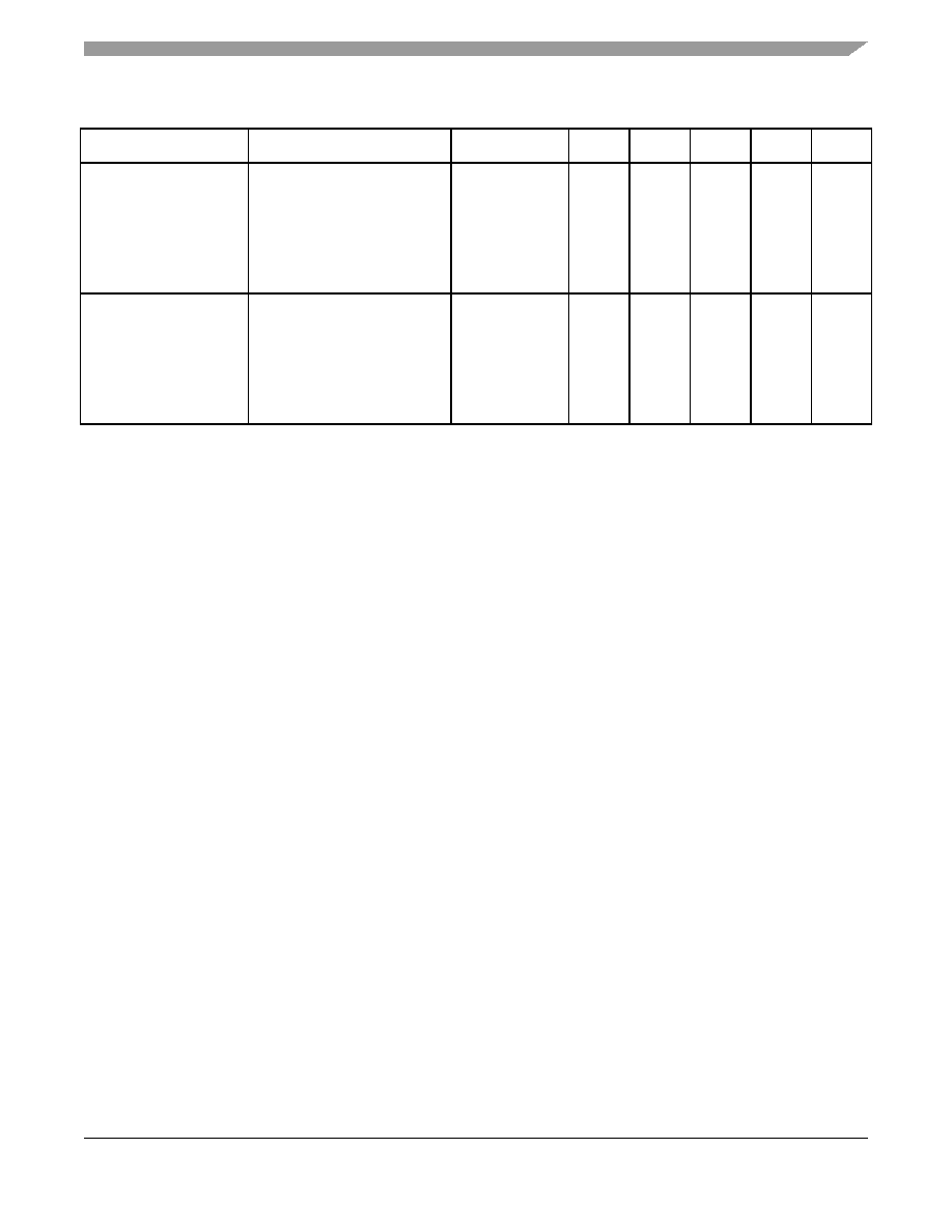
Total Skew
Skew across all lanes on a link.
This includes variation in the
length of SKP ordered set (e.g.
COM and one to five SKP
Symbols) at the Rx as well as
any delay differences arising
from the interconnect itself.
LRX-SKEW
—
20
ns
—
Notes:
1. No test load is necessarily associated with this value.
2. Specified at the measurement point and measured over any 250 consecutive UIs. The test load in Figure 44 should be used
as the Rx device when taking measurements (also refer to the receiver compliance eye diagram shown in Figure 43). If the
clocks to the Rx and Tx are not derived from the same reference clock, the Tx UI recovered from 3500 consecutive UI must
be used as a reference for the eye diagram.
3. A TRx-EYE = 0.40 UI provides for a total sum of 0.60 UI deterministic and random jitter budget for the transmitter and
interconnect collected any 250 consecutive UIs. The TRx-EYE-MEDIAN-to-MAX-JITTER specification ensures a jitter
distribution in which the median and the maximum deviation from the median is less than half of the total. UI jitter budget
collected over any 250 consecutive Tx UIs. It should be noted that the median is not the same as the mean. The jitter median
describes the point in time where the number of jitter points on either side is approximately equal as opposed to the averaged
time value. If the clocks to the Rx and Tx are not derived from the same reference clock, the Tx UI recovered from 3500
consecutive UI must be used as the reference for the eye diagram.
4. The receiver input impedance will result in a differential return loss greater than or equal to 10 dB with the D+ line biased to
300 mV and the D– line biased to –300 mV and a common mode return loss greater than or equal to 6 dB (no bias required)
over a frequency range of 50 MHz to 1.25 GHz. This input impedance requirement applies to all valid input levels. The
reference impedance for return loss measurements for is 50
Ω to ground for both the D+ and D– line (that is, as measured
by a vector network analyzer with 50-
loss measurement.
5. Impedance during all LTSSM states. When transitioning from a fundamental reset to detect (the initial state of the LTSSM)
there is a 5 ms transition time before receiver termination values must be met on all unconfigured lanes of a port.
6. The Rx DC common mode impedance that exists when no power is present or fundamental reset is asserted. This helps
ensure that the receiver detect circuit does not falsely assume a receiver is powered on when it is not. This term must be
measured at 300 mV above the Rx ground.
7. It is recommended that the recovered Tx UI is calculated using all edges in the 3500 consecutive UI interval with a fit algorithm
using a minimization merit function. Least squares and median deviation fits have worked well with experimental and
simulated data.
Table 53. Differential Receiver (Rx) Input Specifications (continued)
Parameter
Comments
Symbol
Min
Typical
Max
Units
Note
相关PDF资料 |
PDF描述 |
|---|---|
| MPC8245TZU266D | IC MPU 32BIT 266MHZ PPC 352-TBGA |
| MPC860DECZQ50D4 | IC MPU PWRQUICC 50MHZ 357-PBGA |
| MPC860DECVR50D4 | IC MPU POWERQUICC 50MHZ 357PBGA |
| 15-47-4143 | CONN FFC FEMALE 14POS.100 GOLD |
| 15-47-4140 | CONN FFC FEMALE 14POS .100 GOLD |
相关代理商/技术参数 |
参数描述 |
|---|---|
| MPC8377VRANDA | 制造商:FREESCALE 制造商全称:Freescale Semiconductor, Inc 功能描述:PowerQUICC? II Pro Processor Hardware Specifications |
| MPC8377VRANFA | 制造商:FREESCALE 制造商全称:Freescale Semiconductor, Inc 功能描述:PowerQUICC? II Pro Processor Hardware Specifications |
| MPC8377VRANG | 功能描述:微处理器 - MPU 837X Non-Encrypted RoHS:否 制造商:Atmel 处理器系列:SAMA5D31 核心:ARM Cortex A5 数据总线宽度:32 bit 最大时钟频率:536 MHz 程序存储器大小:32 KB 数据 RAM 大小:128 KB 接口类型:CAN, Ethernet, LIN, SPI,TWI, UART, USB 工作电源电压:1.8 V to 3.3 V 最大工作温度:+ 85 C 安装风格:SMD/SMT 封装 / 箱体:FBGA-324 |
| MPC8377VRANGA | 功能描述:微处理器 - MPU 8377 PBGA ST PbFr No ENC RoHS:否 制造商:Atmel 处理器系列:SAMA5D31 核心:ARM Cortex A5 数据总线宽度:32 bit 最大时钟频率:536 MHz 程序存储器大小:32 KB 数据 RAM 大小:128 KB 接口类型:CAN, Ethernet, LIN, SPI,TWI, UART, USB 工作电源电压:1.8 V to 3.3 V 最大工作温度:+ 85 C 安装风格:SMD/SMT 封装 / 箱体:FBGA-324 |
| MPC8377ZQAFDA | 制造商:FREESCALE 制造商全称:Freescale Semiconductor, Inc 功能描述:PowerQUICC? II Pro Processor Hardware Specifications |
发布紧急采购,3分钟左右您将得到回复。