- 您现在的位置:买卖IC网 > PDF目录3935 > MPC8536BVTAQGA (Freescale Semiconductor)MPU POWERQUICC III 783FCPBGA PDF资料下载
参数资料
| 型号: | MPC8536BVTAQGA |
| 厂商: | Freescale Semiconductor |
| 文件页数: | 52/126页 |
| 文件大小: | 0K |
| 描述: | MPU POWERQUICC III 783FCPBGA |
| 标准包装: | 1 |
| 系列: | MPC85xx |
| 处理器类型: | 32-位 MPC85xx PowerQUICC III |
| 速度: | 1.0GHz |
| 电压: | 1V |
| 安装类型: | 表面贴装 |
| 封装/外壳: | 783-BBGA,FCBGA |
| 供应商设备封装: | 783-FCPBGA(29x29) |
| 包装: | 托盘 |
第1页第2页第3页第4页第5页第6页第7页第8页第9页第10页第11页第12页第13页第14页第15页第16页第17页第18页第19页第20页第21页第22页第23页第24页第25页第26页第27页第28页第29页第30页第31页第32页第33页第34页第35页第36页第37页第38页第39页第40页第41页第42页第43页第44页第45页第46页第47页第48页第49页第50页第51页当前第52页第53页第54页第55页第56页第57页第58页第59页第60页第61页第62页第63页第64页第65页第66页第67页第68页第69页第70页第71页第72页第73页第74页第75页第76页第77页第78页第79页第80页第81页第82页第83页第84页第85页第86页第87页第88页第89页第90页第91页第92页第93页第94页第95页第96页第97页第98页第99页第100页第101页第102页第103页第104页第105页第106页第107页第108页第109页第110页第111页第112页第113页第114页第115页第116页第117页第118页第119页第120页第121页第122页第123页第124页第125页第126页
Electrical Characteristics
MPC8536E PowerQUICC III Integrated Processor Hardware Specifications, Rev. 5
Freescale Semiconductor
31
2.4.6
Platform to FIFO Restrictions
Please note the following FIFO maximum speed restrictions based on platform speed. The “platform clock (CCB) frequency”
in the following formula refers to the maximum platform (CCB) frequency of the speed bins the part belongs to, which is
defined in Table 73.
For FIFO GMII mode:
FIFO TX/RX clock frequency <= platform clock frequency/3.2
For example, if the platform frequency is 533 MHz, the FIFO TX/RX clock frequency should be no more than 167 MHz
For FIFO encoded mode:
FIFO TX/RX clock frequency <= platform clock frequency/3.2
For example, if the platform frequency is 533 MHz, the FIFO TX/RX clock frequency should be no more than
167 MHz
2.4.7
Other Input Clocks
For information on the input clocks of other functional blocks of the platform such as SerDes, and eTSEC, see the specific
section of this document.
2.5
RESET Initialization
This section describes the AC electrical specifications for the RESET initialization timing requirements of the chip. This table
provides the RESET initialization AC timing specifications for the DDR SDRAM component(s).
This table provides the PLL lock times.
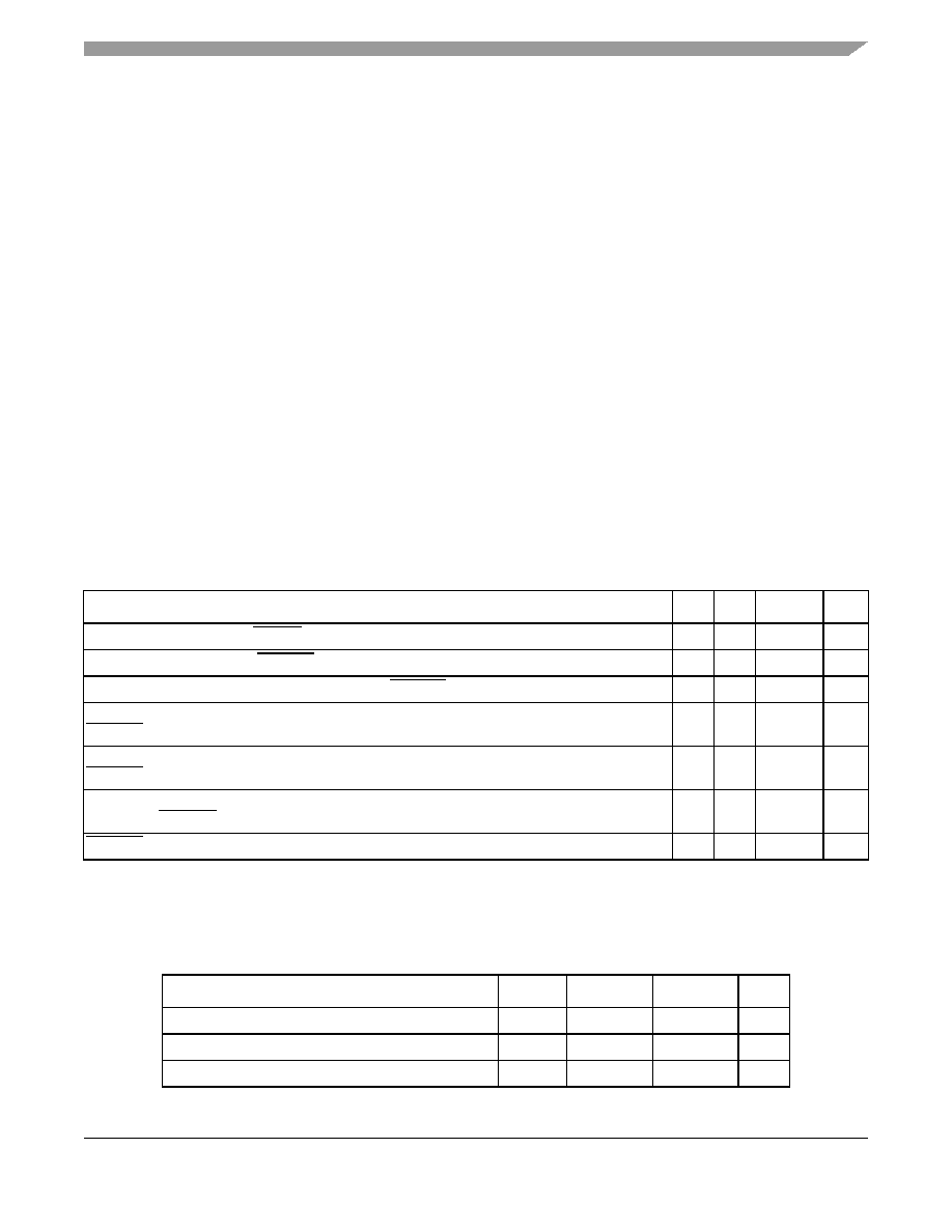
Table 10. RESET Initialization Timing Specifications
Parameter/Condition
Min
Max
Unit
Notes
Required assertion time of HREST
100
—
μs—
Minimum assertion time for SRESET
3—
Sysclk
1
PLL input setup time with stable SYSCLK before HRESET negation
100
—
μs—
Input setup time for POR configurations (other than PLL config) with respect to negation of
HRESET
4
—
SYSCLKs
1
Input hold time for all POR configurations (including PLL config) with respect to negation of
HRESET
2
—
SYSCLKs
1
Maximum valid-to-high impedance time for actively driven POR configurations with respect to
negation of HRESET
—
5
SYSCLKs
1
HRESET rise time
—
1
SYSCLK
—
Notes:
1. SYSCLK is the primary clock input for the chip.
Table 11. PLL Lock Times
Parameter/Condition
Min
Max
Unit
Notes
PLL lock times
—
100
μs—
Local bus PLL
—
50
μs—
PCI bus lock time
—
50
μs—
相关PDF资料 |
PDF描述 |
|---|---|
| MPC8535ECVTAQGA | MPU POWERQUICC III 783FCPBGA |
| CAT25128YI-GT3 | IC EEPROM 128KB SPI SER 8TSSOP |
| 346-020-522-204 | CARDEDGE 20POS DUAL .125 GREEN |
| 346-020-522-202 | CARDEDGE 20POS DUAL .125 GREEN |
| 346-020-522-201 | CARDEDGE 20POS DUAL .125 GREEN |
相关代理商/技术参数 |
参数描述 |
|---|---|
| MPC8536BVTATH | 功能描述:微处理器 - MPU 8536 INDUSTRIAL 1250 RoHS:否 制造商:Atmel 处理器系列:SAMA5D31 核心:ARM Cortex A5 数据总线宽度:32 bit 最大时钟频率:536 MHz 程序存储器大小:32 KB 数据 RAM 大小:128 KB 接口类型:CAN, Ethernet, LIN, SPI,TWI, UART, USB 工作电源电压:1.8 V to 3.3 V 最大工作温度:+ 85 C 安装风格:SMD/SMT 封装 / 箱体:FBGA-324 |
| MPC8536BVTATHA | 功能描述:微处理器 - MPU 8536 Non E RoHS:否 制造商:Atmel 处理器系列:SAMA5D31 核心:ARM Cortex A5 数据总线宽度:32 bit 最大时钟频率:536 MHz 程序存储器大小:32 KB 数据 RAM 大小:128 KB 接口类型:CAN, Ethernet, LIN, SPI,TWI, UART, USB 工作电源电压:1.8 V to 3.3 V 最大工作温度:+ 85 C 安装风格:SMD/SMT 封装 / 箱体:FBGA-324 |
| MPC8536BVTATLA | 功能描述:微处理器 - MPU 8536 NON E RoHS:否 制造商:Atmel 处理器系列:SAMA5D31 核心:ARM Cortex A5 数据总线宽度:32 bit 最大时钟频率:536 MHz 程序存储器大小:32 KB 数据 RAM 大小:128 KB 接口类型:CAN, Ethernet, LIN, SPI,TWI, UART, USB 工作电源电压:1.8 V to 3.3 V 最大工作温度:+ 85 C 安装风格:SMD/SMT 封装 / 箱体:FBGA-324 |
| MPC8536BVTAUL | 功能描述:微处理器 - MPU 8536 INDUSTRIAL 1333 RoHS:否 制造商:Atmel 处理器系列:SAMA5D31 核心:ARM Cortex A5 数据总线宽度:32 bit 最大时钟频率:536 MHz 程序存储器大小:32 KB 数据 RAM 大小:128 KB 接口类型:CAN, Ethernet, LIN, SPI,TWI, UART, USB 工作电源电压:1.8 V to 3.3 V 最大工作温度:+ 85 C 安装风格:SMD/SMT 封装 / 箱体:FBGA-324 |
| MPC8536BVTAULA | 功能描述:微处理器 - MPU 8536 Non E RoHS:否 制造商:Atmel 处理器系列:SAMA5D31 核心:ARM Cortex A5 数据总线宽度:32 bit 最大时钟频率:536 MHz 程序存储器大小:32 KB 数据 RAM 大小:128 KB 接口类型:CAN, Ethernet, LIN, SPI,TWI, UART, USB 工作电源电压:1.8 V to 3.3 V 最大工作温度:+ 85 C 安装风格:SMD/SMT 封装 / 箱体:FBGA-324 |
发布紧急采购,3分钟左右您将得到回复。