- 您现在的位置:买卖IC网 > PDF目录45372 > MPC8569ECVTANKG (FREESCALE SEMICONDUCTOR INC) RISC PROCESSOR, PBGA783 PDF资料下载
参数资料
| 型号: | MPC8569ECVTANKG |
| 厂商: | FREESCALE SEMICONDUCTOR INC |
| 元件分类: | 微控制器/微处理器 |
| 英文描述: | RISC PROCESSOR, PBGA783 |
| 封装: | 29 X 29 MM, 1 MM PITCH, PLASTIC, BGA-783 |
| 文件页数: | 99/126页 |
| 文件大小: | 2847K |
| 代理商: | MPC8569ECVTANKG |
第1页第2页第3页第4页第5页第6页第7页第8页第9页第10页第11页第12页第13页第14页第15页第16页第17页第18页第19页第20页第21页第22页第23页第24页第25页第26页第27页第28页第29页第30页第31页第32页第33页第34页第35页第36页第37页第38页第39页第40页第41页第42页第43页第44页第45页第46页第47页第48页第49页第50页第51页第52页第53页第54页第55页第56页第57页第58页第59页第60页第61页第62页第63页第64页第65页第66页第67页第68页第69页第70页第71页第72页第73页第74页第75页第76页第77页第78页第79页第80页第81页第82页第83页第84页第85页第86页第87页第88页第89页第90页第91页第92页第93页第94页第95页第96页第97页第98页当前第99页第100页第101页第102页第103页第104页第105页第106页第107页第108页第109页第110页第111页第112页第113页第114页第115页第116页第117页第118页第119页第120页第121页第122页第123页第124页第125页第126页
MPC8569E PowerQUICC III Integrated Processor Hardware Specifications, Rev. 0
Ethernet Management Interface
Freescale Semiconductor
74
2.7.1.1
MII Management AC Electrical Specifications
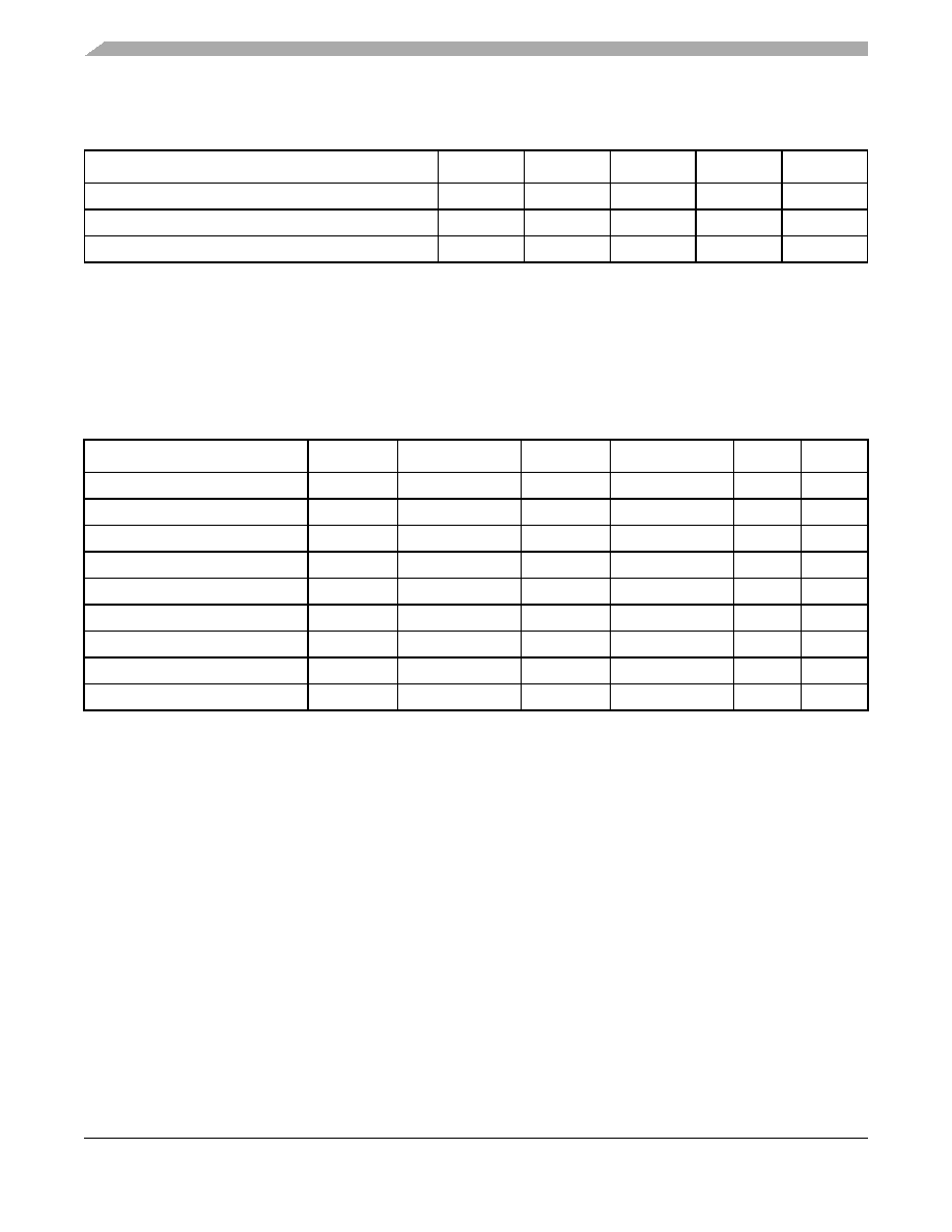
The following table provides the MII management AC timing specifications.
Input low current (LVDD = Max, VIN = 0.5 V)
IIL
–600
—
μA1
Output high voltage (LVDD = Min, IOH = –4.0 mA)
VOH
2.4
—
V
—
Output low voltage (LVDD = Min, IOL = 4.0 mA)
VOL
—0.4
V
—
Note:
Table 42. MII Management AC Timing Specifications
At recommended operating conditions with LVDD = 3.3 V ± 5%.
Parameter
Symbol1
Min
Typ
Max
Unit
Notes
MDC frequency
fMDC
—2.5
—
MHz
2
MDC period
tMDC
—400
—
ns
—
MDC clock pulse width high
tMDCH
32
—
ns
—
MDC to MDIO valid
tMDKHDV
2
× (tplb_clk*8)
—
ns
4
MDC to MDIO delay
tMDKHDX
(16
× tplb_clk) – 3
—
(16
× tplb_clk) + 3
ns
3, 4, 5
MDIO to MDC setup time
tMDDVKH
10
—
ns
—
MDIO to MDC hold time
tMDDXKH
0—
—
ns
—
MDC rise time
tMDCR
—
10
ns
—
MDC fall time
tMDCF
—
10
ns
—
Notes:
1. The symbols used for timing specifications follow the pattern of t(first two letters of functional block)(signal)(state)(reference)(state) for
inputs and t(first two letters of functional block)(reference)(state)(signal)(state) for outputs. For example, tMDKHDX symbolizes management
data timing (MD) for the time tMDC from clock reference (K) high (H) until data outputs (D) are invalid (X) or data hold time.
Also, tMDDVKH symbolizes management data timing (MD) with respect to the time data input signals (D) reaching the valid
state (V) relative to the tMDC clock reference (K) going to the high (H) state or setup time. For rise and fall times, the latter
convention is used with the appropriate letter: R (rise) or F (fall).
2. This parameter is dependent on the platform clock frequency (MIIMCFG [MgmtClk] field determines the clock frequency of
the Mgmt Clock CE_MDC).
3. This parameter is dependent on the platform clock frequency. The delay is equal to 16 platform clock periods ±3 ns. For
example, with a platform clock of 400 MHz, the min/max delay is 40 ns ± 3 ns.
4. tplb_clk is the QUICC Engine block clock/2.
5. MDC to MDIO Data valid tMDKHDV is a function of clock period and max delay time (tMDKHDX).
(Min setup = cycle time – max delay
Table 41. MII Management DC Electrical Characteristics (continued)
At recommended operating conditions with LVDD = 3.3 V
Parameter
Symbol
Min
Max
Unit
Notes
相关PDF资料 |
PDF描述 |
|---|---|
| MPC8569VTAUNLA | RISC PROCESSOR, PBGA783 |
| MPC8569EVTAUNL | RISC PROCESSOR, PBGA783 |
| MPC8569ECVTAQLJA | RISC PROCESSOR, PBGA783 |
| MPC8569EVTANKGB | RISC PROCESSOR, PBGA783 |
| MPC8569EVTAQLJA | RISC PROCESSOR, PBGA783 |
相关代理商/技术参数 |
参数描述 |
|---|---|
| MPC8569ECVTANKGB | 功能描述:数字信号处理器和控制器 - DSP, DSC 8569E XT 800/600/400 r2.1 RoHS:否 制造商:Microchip Technology 核心:dsPIC 数据总线宽度:16 bit 程序存储器大小:16 KB 数据 RAM 大小:2 KB 最大时钟频率:40 MHz 可编程输入/输出端数量:35 定时器数量:3 设备每秒兆指令数:50 MIPs 工作电源电压:3.3 V 最大工作温度:+ 85 C 封装 / 箱体:TQFP-44 安装风格:SMD/SMT |
| MPC8569ECVTAQLJB | 功能描述:数字信号处理器和控制器 - DSP, DSC 8569E XT1067/667/533 r2.1 RoHS:否 制造商:Microchip Technology 核心:dsPIC 数据总线宽度:16 bit 程序存储器大小:16 KB 数据 RAM 大小:2 KB 最大时钟频率:40 MHz 可编程输入/输出端数量:35 定时器数量:3 设备每秒兆指令数:50 MIPs 工作电源电压:3.3 V 最大工作温度:+ 85 C 封装 / 箱体:TQFP-44 安装风格:SMD/SMT |
| MPC8569E-MDS-PB | 功能描述:开发板和工具包 - 其他处理器 MPC8569 MDS PROCESSOR BD RoHS:否 制造商:Freescale Semiconductor 产品:Development Systems 工具用于评估:P3041 核心:e500mc 接口类型:I2C, SPI, USB 工作电源电压: |
| MPC8569EVTANKGB | 功能描述:数字信号处理器和控制器 - DSP, DSC 8569 800MHz rev2.1 RoHS:否 制造商:Microchip Technology 核心:dsPIC 数据总线宽度:16 bit 程序存储器大小:16 KB 数据 RAM 大小:2 KB 最大时钟频率:40 MHz 可编程输入/输出端数量:35 定时器数量:3 设备每秒兆指令数:50 MIPs 工作电源电压:3.3 V 最大工作温度:+ 85 C 封装 / 箱体:TQFP-44 安装风格:SMD/SMT |
| MPC8569EVTAQLJB | 功能描述:数字信号处理器和控制器 - DSP, DSC 8569 1GHz rev2.1 RoHS:否 制造商:Microchip Technology 核心:dsPIC 数据总线宽度:16 bit 程序存储器大小:16 KB 数据 RAM 大小:2 KB 最大时钟频率:40 MHz 可编程输入/输出端数量:35 定时器数量:3 设备每秒兆指令数:50 MIPs 工作电源电压:3.3 V 最大工作温度:+ 85 C 封装 / 箱体:TQFP-44 安装风格:SMD/SMT |
发布紧急采购,3分钟左右您将得到回复。