- 您现在的位置:买卖IC网 > PDF目录45372 > MPC8569ECVTANKGB (FREESCALE SEMICONDUCTOR INC) RISC PROCESSOR, PBGA783 PDF资料下载
参数资料
| 型号: | MPC8569ECVTANKGB |
| 厂商: | FREESCALE SEMICONDUCTOR INC |
| 元件分类: | 微控制器/微处理器 |
| 英文描述: | RISC PROCESSOR, PBGA783 |
| 封装: | 29 X 29 MM, 1 MM PITCH, PLASTIC, BGA-783 |
| 文件页数: | 112/126页 |
| 文件大小: | 2847K |
| 代理商: | MPC8569ECVTANKGB |
第1页第2页第3页第4页第5页第6页第7页第8页第9页第10页第11页第12页第13页第14页第15页第16页第17页第18页第19页第20页第21页第22页第23页第24页第25页第26页第27页第28页第29页第30页第31页第32页第33页第34页第35页第36页第37页第38页第39页第40页第41页第42页第43页第44页第45页第46页第47页第48页第49页第50页第51页第52页第53页第54页第55页第56页第57页第58页第59页第60页第61页第62页第63页第64页第65页第66页第67页第68页第69页第70页第71页第72页第73页第74页第75页第76页第77页第78页第79页第80页第81页第82页第83页第84页第85页第86页第87页第88页第89页第90页第91页第92页第93页第94页第95页第96页第97页第98页第99页第100页第101页第102页第103页第104页第105页第106页第107页第108页第109页第110页第111页当前第112页第113页第114页第115页第116页第117页第118页第119页第120页第121页第122页第123页第124页第125页第126页
MPC8569E PowerQUICC III Integrated Processor Hardware Specifications, Rev. 0
PCI Express
Freescale Semiconductor
86
2.10.3
PCI Express AC Physical Layer Specifications
This section contains the DC specifications for the physical layer of PCI Express on this device.
2.10.3.1
PCI Express AC Physical Layer Transmitter Specifications
This section discusses the PCI Express AC physical layer transmitter specifications for 2.5 Gb/s.
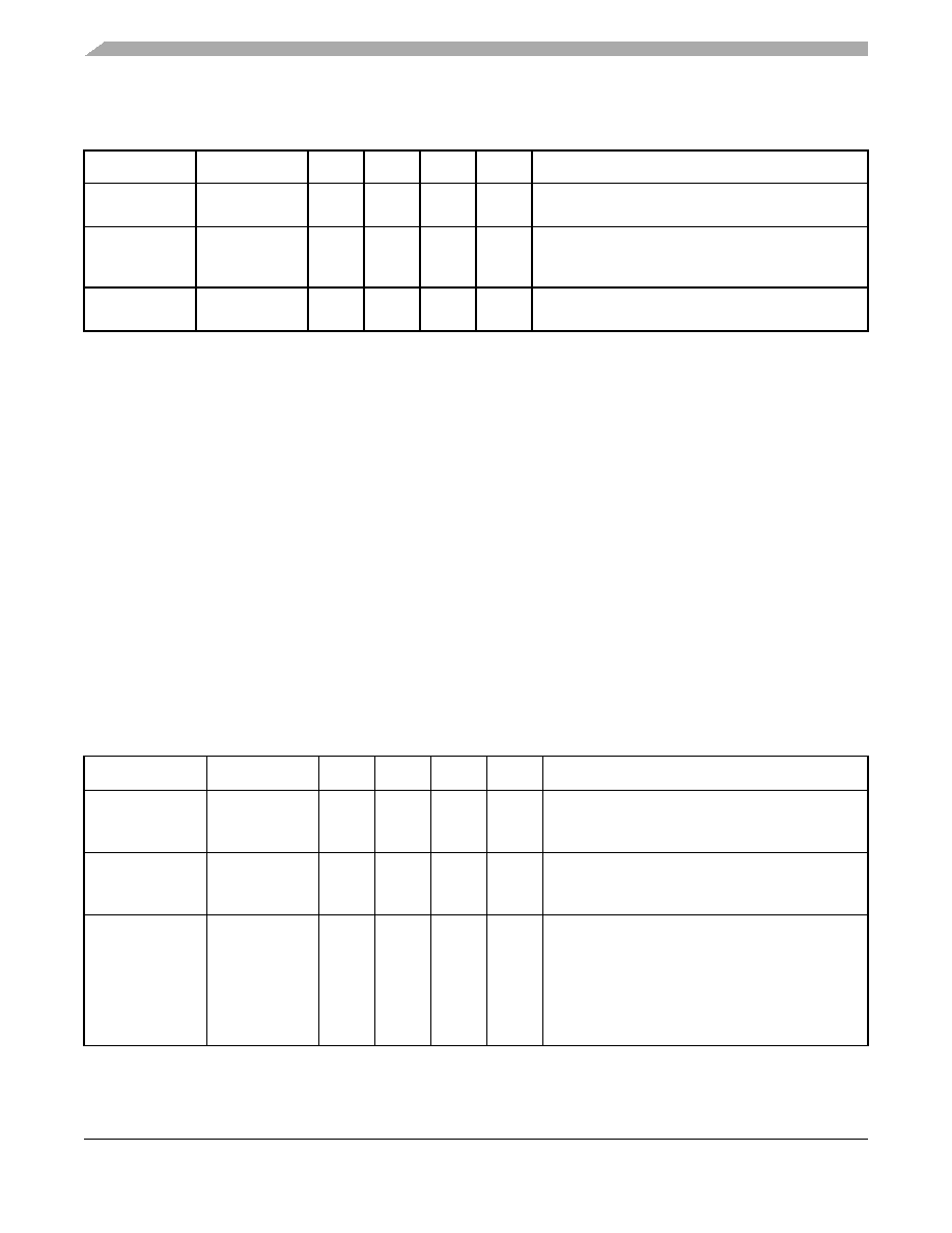
The following table defines the PCI Express (2.5Gb/s) AC specifications for the differential output at all transmitters (TXs). The
parameters are specified at the component pins. The AC timing specifications do not include RefClk jitter.
DC input
impedance
ZRX-DC
40
50
60
Ω
Required RX D+ as well as D– DC impedance
(50 ± 20% tolerance). See Notes 1 and 2.
Powered down
DC input
impedance
ZRX-HIGH-IMP-DC
50
—
ΚΩ
Required RX D+ as well as D– DC Impedance when
the receiver terminations do not have power. See Note
3.
Electrical idle
detect threshold
VRX-IDLE-DET-
DIFFp-p
65
—
175
mV
VRX-IDLE-DET-DIFFp-p = 2 × |VRX-D+ – VRX-D–|.
Measured at the package pins of the receiver.
Notes:
1. Specified at the measurement point and measured over any 250 consecutive UIs. The test load in Figure 46 must be used
as the RX device when taking measurements. If the clocks to the RX and TX are not derived from the same reference clock,
the TX UI recovered from 3500 consecutive UI must be used as a reference for the eye diagram.
2. Impedance during all LTSSM states. When transitioning from a fundamental reset to detect (the initial state of the LTSSM)
there is a 5 ms transition time before receiver termination values must be met on all unconfigured lanes of a port.
3. The RX DC common mode impedance that exists when no power is present or fundamental reset is asserted. This helps
ensure that the receiver detect circuit will not falsely assume a receiver is powered on when it is not. This term must be
measured at 300 mV above the RX ground.
Table 50. PCI Express (2.5Gb/s) Differential Transmitter (TX) Output AC Specifications
At recommended operating conditions with XVDD = 1.0 V ± 3%. and 1.1 V ± 3%
Parameter
Symbol
Min
Typ
Max
Unit
Comments
Unit Interval
UI
399.88
400.00
400.12
ps
Each UI is 400 ps ± 300 ppm. UI does not account
for spread spectrum clock dictated variations. See
Note 1.
Minimum TX eye
width
TTX-EYE
0.70
—
UI
The maximum transmitter jitter can be derived as
TTX-MAX-JITTER = 1 – TTX-EYE = 0.3 UI.
See Notes 2 and 3.
Maximum time
between the jitter
median and
maximum
deviation from the
median
TTX-EYE-MEDIAN-
to-MAX-JITTER
—
0.15
UI
Jitter is defined as the measurement variation of the
crossing points (VTX-DIFFp-p = 0 V) in relation to a
recovered TX UI. A recovered TX UI is calculated
over 3500 consecutive unit intervals of sample data.
Jitter is measured using all edges of the 250
consecutive UI in the center of the 3500 UI used for
calculating the TX UI. See Notes 2 and 3.
Table 49. PCI Express (2.5 Gb/s) Differential Receiver (RX) Input DC Specifications (continued)
At recommended operating conditions with ScoreVDD = 1.0 V ± 3%. and 1.1 V ± 3%
Parameter
Symbol
Min
Typ
Max
Unit
Comments
相关PDF资料 |
PDF描述 |
|---|---|
| MPC8569ECVTANKG | RISC PROCESSOR, PBGA783 |
| MPC8569VTAUNLA | RISC PROCESSOR, PBGA783 |
| MPC8569EVTAUNL | RISC PROCESSOR, PBGA783 |
| MPC8569ECVTAQLJA | RISC PROCESSOR, PBGA783 |
| MPC8569EVTANKGB | RISC PROCESSOR, PBGA783 |
相关代理商/技术参数 |
参数描述 |
|---|---|
| MPC8569ECVTAQLJB | 功能描述:数字信号处理器和控制器 - DSP, DSC 8569E XT1067/667/533 r2.1 RoHS:否 制造商:Microchip Technology 核心:dsPIC 数据总线宽度:16 bit 程序存储器大小:16 KB 数据 RAM 大小:2 KB 最大时钟频率:40 MHz 可编程输入/输出端数量:35 定时器数量:3 设备每秒兆指令数:50 MIPs 工作电源电压:3.3 V 最大工作温度:+ 85 C 封装 / 箱体:TQFP-44 安装风格:SMD/SMT |
| MPC8569E-MDS-PB | 功能描述:开发板和工具包 - 其他处理器 MPC8569 MDS PROCESSOR BD RoHS:否 制造商:Freescale Semiconductor 产品:Development Systems 工具用于评估:P3041 核心:e500mc 接口类型:I2C, SPI, USB 工作电源电压: |
| MPC8569EVTANKGB | 功能描述:数字信号处理器和控制器 - DSP, DSC 8569 800MHz rev2.1 RoHS:否 制造商:Microchip Technology 核心:dsPIC 数据总线宽度:16 bit 程序存储器大小:16 KB 数据 RAM 大小:2 KB 最大时钟频率:40 MHz 可编程输入/输出端数量:35 定时器数量:3 设备每秒兆指令数:50 MIPs 工作电源电压:3.3 V 最大工作温度:+ 85 C 封装 / 箱体:TQFP-44 安装风格:SMD/SMT |
| MPC8569EVTAQLJB | 功能描述:数字信号处理器和控制器 - DSP, DSC 8569 1GHz rev2.1 RoHS:否 制造商:Microchip Technology 核心:dsPIC 数据总线宽度:16 bit 程序存储器大小:16 KB 数据 RAM 大小:2 KB 最大时钟频率:40 MHz 可编程输入/输出端数量:35 定时器数量:3 设备每秒兆指令数:50 MIPs 工作电源电压:3.3 V 最大工作温度:+ 85 C 封装 / 箱体:TQFP-44 安装风格:SMD/SMT |
| MPC8569EVTAUNLB | 功能描述:数字信号处理器和控制器 - DSP, DSC 8569 1.33GHz rev2.1 RoHS:否 制造商:Microchip Technology 核心:dsPIC 数据总线宽度:16 bit 程序存储器大小:16 KB 数据 RAM 大小:2 KB 最大时钟频率:40 MHz 可编程输入/输出端数量:35 定时器数量:3 设备每秒兆指令数:50 MIPs 工作电源电压:3.3 V 最大工作温度:+ 85 C 封装 / 箱体:TQFP-44 安装风格:SMD/SMT |
发布紧急采购,3分钟左右您将得到回复。