- 您现在的位置:买卖IC网 > PDF目录2014 > MPC92439EI (IDT, Integrated Device Technology Inc)IC SYNTHESIZER LVPECL 28-PLCC PDF资料下载
参数资料
| 型号: | MPC92439EI |
| 厂商: | IDT, Integrated Device Technology Inc |
| 文件页数: | 16/16页 |
| 文件大小: | 0K |
| 描述: | IC SYNTHESIZER LVPECL 28-PLCC |
| 标准包装: | 37 |
| 类型: | 时钟/频率合成器 |
| PLL: | 是 |
| 输入: | 晶体 |
| 输出: | LVPECL |
| 电路数: | 1 |
| 比率 - 输入:输出: | 1:1 |
| 差分 - 输入:输出: | 无/是 |
| 频率 - 最大: | 900MHz |
| 除法器/乘法器: | 是/无 |
| 电源电压: | 3.135 V ~ 3.465 V |
| 工作温度: | 0°C ~ 70°C |
| 安装类型: | 表面贴装 |
| 封装/外壳: | 28-LCC(J 形引线) |
| 供应商设备封装: | 28-PLCC(11.5x11.5) |
| 包装: | 管件 |
MPC92439 Data Sheet
900MHZ, LOW VOLTAGE, LVPECL CLOCK SYNTHESIZER
MPC92439 REVISION 5 FEBRUARY 6, 2013
9
2013 Integrated Device Technology, Inc.
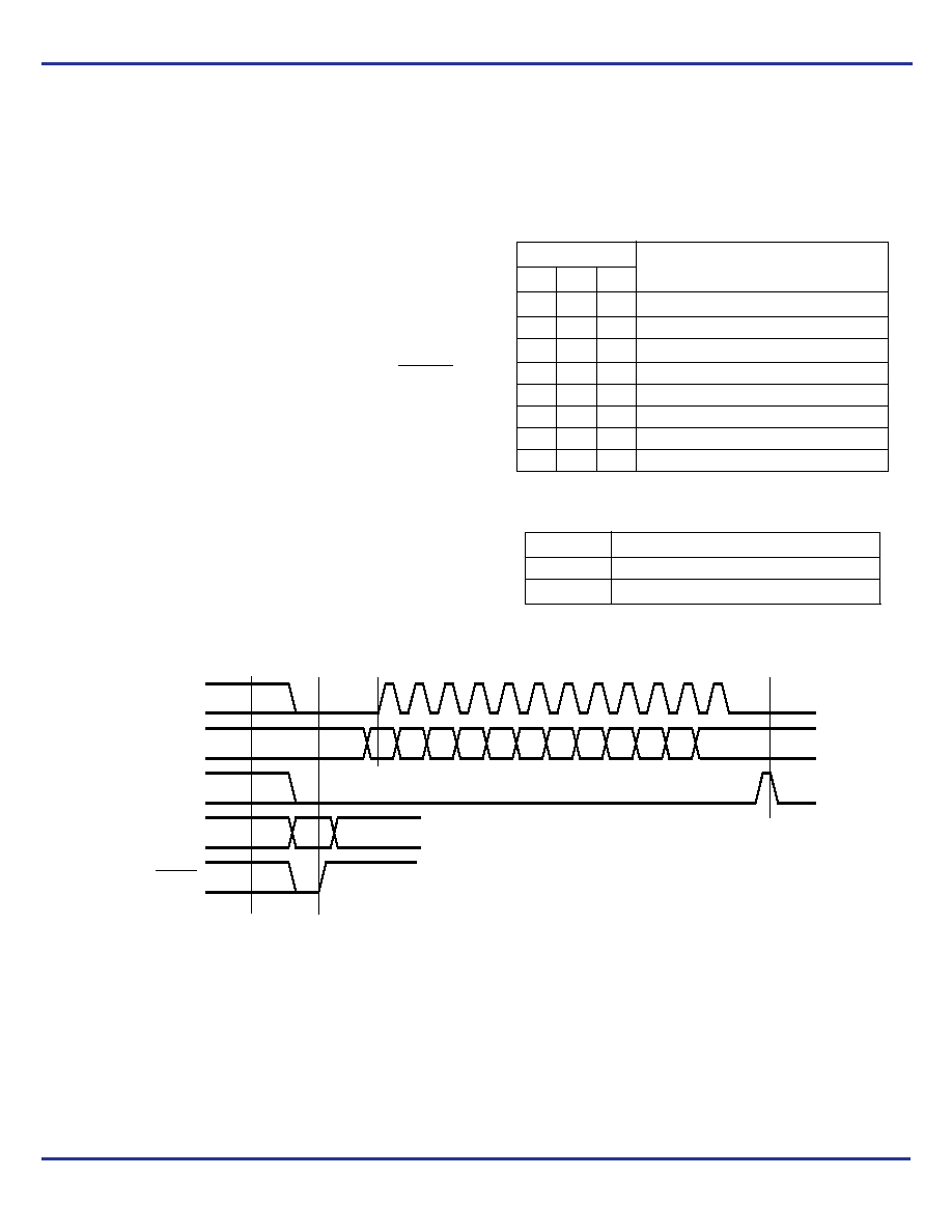
transition on the S_LOAD input will latch the new divide values into
the counters. Figure 7 illustrates the timing diagram for both a
parallel and a serial load of the MPC92439 synthesizer.
M[6:0] and N[1:0] are normally specified once at power-up
through the parallel interface, and then possibly again through the
serial interface. This approach allows the application to come up at
one frequency and then change or fine-tune the clock as the ability
to control the serial interface becomes available.
Using the Test and Diagnosis Output TEST
The TEST output provides visibility for one of the several internal
nodes as determined by the T[2:0] bits in the serial configuration
stream. It is not configurable through the parallel interface. Although
it is possible to select the node that represents FOUT, the LVCMOS
output is not able to toggle fast enough for higher output frequencies
and should only be used for test and diagnosis.
The T2, T1 and T0 control bits are preset to ‘000' when P_LOAD
is LOW so that the PECL FOUT outputs are as jitter-free as possible.
Any active signal on the TEST output pin will have detrimental
affects on the jitter of the PECL output pair. In normal operations,
jitter specifications are only guaranteed if the TEST output is static.
The serial configuration port can be used to select one of the
alternate functions for this pin.
Most of the signals available on the TEST output pin are useful
only for performance verification of the MPC92439 itself. However,
the PLL bypass mode may be of interest at the board level for
functional debug. When T[2:0] is set to 110 the MPC92439 is placed
in PLL bypass mode. In this mode the S_CLOCK input is fed directly
into the M and N dividers. The N divider drives the FOUT differential
pair and the M counter drives the TEST output pin. In this mode the
S_CLOCK input could be used for low speed board level functional
test or debug. Bypassing the PLL and driving FOUT directly gives
the user more control on the test clocks sent through the clocktree
shows the functional setup of the PLL bypass mode. Because the
S_CLOCK is a CMOS level the input frequency is limited to 200
MHz. This means the fastest the FOUT pin can be toggled via the
S_CLOCK is 100 MHz as the divide ratio of the Post-PLL divider is
2 (if N = 1). Note that the M counter output on the TEST output will
not be a 50% duty cycle.
Figure 7. Serial Interface Timing Diagram
Power Supply Filtering
The MPC92439 is a mixed analog/digital product. Its analog
circuitry is naturally susceptible to random noise, especially if this
noise is seen on the power supply pins. Random noise on the
VCC_PLL pin impacts the device characteristics. The MPC92439
provides separate power supplies for the digital circuitry (VCC) and
the internal PLL (VCC_PLL) of the device. The purpose of this design
technique is to try and isolate the high switching noise digital outputs
from the relatively sensitive internal analog phase-locked loop. In a
controlled environment such as an evaluation board, this level of
isolation is sufficient. However, in a digital system environment
where it is more difficult to minimize noise on the power supplies a
second level of isolation may be required. The simplest form of
isolation is a power supply filter on the VCC_PLL pin for the
MPC92439. Figure 8 illustrates a typical power supply filter scheme.
The MPC92439 is most susceptible to noise with spectral content in
the 1 kHz to 1 MHz range. Therefore, the filter should be designed
to target this range. The key parameter that needs to be met in the
final filter design is the DC voltage drop that will be seen between
Table 10. Test and Debug Configuration for TEST
T[2:0]
TEST Output
T2
T1
T0
000
12-bit shift register out(1)
1. Clocked out at the rate of S_CLOCK\
0
1
Logic 1
010
fXTAL 2
0
1
M-Counter out
1
0
FOUT
1
0
1
Logic 0
1
0
M-Counter out in PLL-bypass mode
1
FOUT
4
Table 11. Debug Configuration for PLL Bypass(1)
1. T[2:0] = 110. AC specifications do not apply in PLL bypass
mode
Output
Configuration
FOUT
S_CLOCK
N
TEST
M-Counter out(2)
2. Clocked out at the rate of S_CLOCK
(2N)
S_CLOCK
S_DATA
S_LOAD
M[6:0]
N[1:0]
P_LOAD
T2 T1
T0
N1
N0
M6
M5
M4
M3
M2
M1
M0
M, N
First
Bit
Last
Bit
相关PDF资料 |
PDF描述 |
|---|---|
| MPC9330AC | IC PLL CLOCK GENERATOR 32-LQFP |
| MPC9331AC | IC PLL CLOCK GEN 1:6 32-LQFP |
| MPC9351FA | IC PLL CLOCK DRIVER LV 32-LQFP |
| MPC9352AC | IC CLK GEN ZD 1:11 32-LQFP |
| MPC93H51AC | IC PLL CLK DRIVER LV 32-LQFP |
相关代理商/技术参数 |
参数描述 |
|---|---|
| MPC92439EIR2 | 功能描述:时钟合成器/抖动清除器 FSL 900MHz LVPECL Freq. Synthesizer RoHS:否 制造商:Skyworks Solutions, Inc. 输出端数量: 输出电平: 最大输出频率: 输入电平: 最大输入频率:6.1 GHz 电源电压-最大:3.3 V 电源电压-最小:2.7 V 封装 / 箱体:TSSOP-28 封装:Reel |
| MPC92439FA | 制造商:IDT 制造商全称:Integrated Device Technology 功能描述:900MHz, Low Voltage, LVPECL Clock Syntheesizer |
| MPC92439KLF | 制造商:IDT 制造商全称:Integrated Device Technology 功能描述:900MHz, Low Voltage, LVPECL Clock Syntheesizer |
| MPC92469 | 制造商:IDT 制造商全称:Integrated Device Technology 功能描述:400 MHz Low Voltage PECL Clock Synthesizer w/Spread Spectrum |
| MPC92469AC | 功能描述:时钟合成器/抖动清除器 LVPECL Clock Synthesizer RoHS:否 制造商:Skyworks Solutions, Inc. 输出端数量: 输出电平: 最大输出频率: 输入电平: 最大输入频率:6.1 GHz 电源电压-最大:3.3 V 电源电压-最小:2.7 V 封装 / 箱体:TSSOP-28 封装:Reel |
发布紧急采购,3分钟左右您将得到回复。