- 您现在的位置:买卖IC网 > PDF目录29137 > MPC9352AC (INTEGRATED DEVICE TECHNOLOGY INC) 9352 SERIES, PLL BASED CLOCK DRIVER, 11 TRUE OUTPUT(S), 0 INVERTED OUTPUT(S), PQFP32 PDF资料下载
参数资料
| 型号: | MPC9352AC |
| 厂商: | INTEGRATED DEVICE TECHNOLOGY INC |
| 元件分类: | 时钟及定时 |
| 英文描述: | 9352 SERIES, PLL BASED CLOCK DRIVER, 11 TRUE OUTPUT(S), 0 INVERTED OUTPUT(S), PQFP32 |
| 封装: | LEAD FREE, LQFP-32 |
| 文件页数: | 13/17页 |
| 文件大小: | 367K |
| 代理商: | MPC9352AC |
IDT / ICS 3.3V/2.5V 1:11 LVCMOS ZERO DELAY CLOCK GENERATOR 5
MPC9352
REV 7 MAY 30, 2006
Freescle Timing Solutions Organization has been acquired by Integrated Device Technology, Inc.
MPC9353
3.3V/2.5V 1:11 LVCMOS ZERO DELAY CLOCK GENERATOR
CLOCK GENERATOR
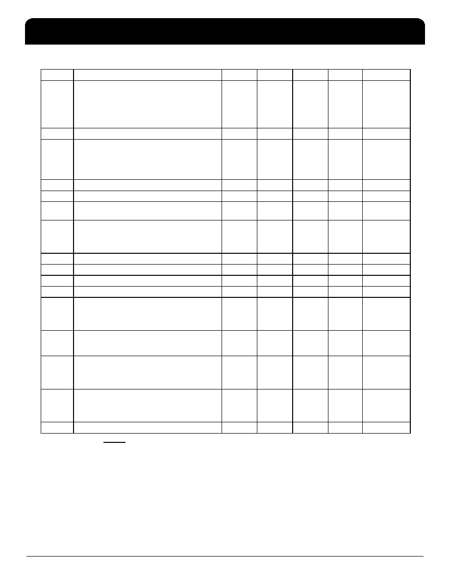
Table 6. AC Characteristics (VCC = 3.3 V ± 5%, TA = –40° to 85°C)(1)
1. AC characteristics apply for parallel output termination of 50
Ω to VTT.
Symbol
Characteristics
Min
Typ
Max
Unit
Condition
fref
Input reference frequency in PLL mode(2)
÷4 feedback
÷6 feedback
÷8 feedback
÷12 feedback
Input reference frequency in PLL bypass mode(3)
2. PLL mode requires PLL_EN=0 to enable the PLL and zero-delay operation. It is not recommended to use a
÷2 divider for feedback.
3. In PLL bypass mode, the MPC9352 divides the input reference clock.
50.0
33.3
25.0
16.67
100.0
66.6
50.0
33.3
250.0
MHz
fVCO
VCO lock frequency range(4)
4. The input frequency fref on CCLK must match the VCO frequency range divided by the feedback divider ratio FB: fref = fVCO ÷ FB.
200
400
MHz
fMAX
Output Frequency
÷2 output(5)
÷4 output
÷6 output
÷8 output
÷12 output
100
50
33.3
25
16.67
200
100
66.6
50
33.3
MHz
frefDC
Reference Input Duty Cycle
25
75
%
tr, tf
CCLK Input Rise/Fall Time
1.0
ns
0.8 to 2.0 V
t()
Propagation Delay CCLK to FB_IN
fref > 40 MHz
(static phase offset)
fref < 40 MHz
–50
–200
+150
ps
PLL locked
tsk(O)
Output-to-output Skew(6)
all outputs, any frequency
within QA output bank
within QB output bank
within QC output bank
6. See Applications Information section for part-to-part skew calculation.
200
100
ps
DC
Output duty cycle
47
50
53
%
tr, tf
Output Rise/Fall Time
0.1
1.0
ns
0.55 to 2.4 V
tPLZ, HZ
Output Disable Time
8
ns
tPZL, LZ
Output Enable Time
10
ns
tJIT(CC)
Cycle-to-cycle jitter
output frequencies mixed
outputs are in any
÷4 and ÷6 combination
all outputs same frequency
400
250
100
ps
tJIT(PER) Period Jitter
output frequencies mixed
outputs are in any
÷4 and ÷6 combination
all outputs same frequency
200
150
75
ps
tJIT()
I/O Phase Jitter
÷4 feedback divider RMS (1 σ)(7)
÷6 feedback divider RMS (1 σ)
÷8 feedback divider RMS (1 σ)
÷12 feedback divider RMS (1 σ)
7. See Applications Information section for a jitter calculation for other confidence factors than 1
σ.
15
20
18 – 20
25
ps
BW
PLL closed loop bandwidth(8)
÷4 feedback
÷6 feedback
÷8 feedback
÷12 feedback
8. -3 dB point of PLL transfer characteristics.
3.0 – 10.0
1.5 – 6.0
1.0 – 3.5
0.5 – 2.0
MHz
tLOCK
Maximum PLL Lock Time
10
ms
相关PDF资料 |
PDF描述 |
|---|---|
| MPC93H52ACR2 | 93H SERIES, PLL BASED CLOCK DRIVER, 11 TRUE OUTPUT(S), 0 INVERTED OUTPUT(S), PQFP32 |
| MPC93R51FAR2 | 93R SERIES, PLL BASED CLOCK DRIVER, 9 TRUE OUTPUT(S), 0 INVERTED OUTPUT(S), PQFP32 |
| MPC93R51FA | 93R SERIES, PLL BASED CLOCK DRIVER, 9 TRUE OUTPUT(S), 0 INVERTED OUTPUT(S), PQFP32 |
| MPC93R51ACR2 | 93R SERIES, PLL BASED CLOCK DRIVER, 9 TRUE OUTPUT(S), 0 INVERTED OUTPUT(S), PQFP32 |
| MPC940LFAR2 | MPC900 SERIES, LOW SKEW CLOCK DRIVER, 18 TRUE OUTPUT(S), 0 INVERTED OUTPUT(S), PQFP32 |
相关代理商/技术参数 |
参数描述 |
|---|---|
| MPC9352ACR2 | 功能描述:时钟发生器及支持产品 FSL 1-11 LVCMOS PLL Clock Generator RoHS:否 制造商:Silicon Labs 类型:Clock Generators 最大输入频率:14.318 MHz 最大输出频率:166 MHz 输出端数量:16 占空比 - 最大:55 % 工作电源电压:3.3 V 工作电源电流:1 mA 最大工作温度:+ 85 C 安装风格:SMD/SMT 封装 / 箱体:QFN-56 |
| MPC9352FA | 功能描述:锁相环 - PLL 2.5 3.3V 200MHz Clock Generator RoHS:否 制造商:Silicon Labs 类型:PLL Clock Multiplier 电路数量:1 最大输入频率:710 MHz 最小输入频率:0.002 MHz 输出频率范围:0.002 MHz to 808 MHz 电源电压-最大:3.63 V 电源电压-最小:1.71 V 最大工作温度:+ 85 C 最小工作温度:- 40 C 封装 / 箱体:QFN-36 封装:Tray |
| MPC9352FAR2 | 制造商:Integrated Device Technology Inc 功能描述:Zero Delay PLL Clock Generator Single 32-Pin LQFP T/R 制造商:Integrated Device Technology Inc 功能描述:ZERO DLY PLL CLOCK GEN SGL 32LQFP - Tape and Reel |
| MPC93H51AC | 功能描述:时钟发生器及支持产品 FSL 1-9 LVCMOS/LVPEC L to LVCMOS PLL Cloc RoHS:否 制造商:Silicon Labs 类型:Clock Generators 最大输入频率:14.318 MHz 最大输出频率:166 MHz 输出端数量:16 占空比 - 最大:55 % 工作电源电压:3.3 V 工作电源电流:1 mA 最大工作温度:+ 85 C 安装风格:SMD/SMT 封装 / 箱体:QFN-56 |
| MPC93H51ACR2 | 功能描述:时钟发生器及支持产品 FSL 1-9 LVCMOS/LVPEC L to LVCMOS PLL Cloc RoHS:否 制造商:Silicon Labs 类型:Clock Generators 最大输入频率:14.318 MHz 最大输出频率:166 MHz 输出端数量:16 占空比 - 最大:55 % 工作电源电压:3.3 V 工作电源电流:1 mA 最大工作温度:+ 85 C 安装风格:SMD/SMT 封装 / 箱体:QFN-56 |
发布紧急采购,3分钟左右您将得到回复。