- 您现在的位置:买卖IC网 > PDF目录29137 > MPC93H52ACR2 (FREESCALE SEMICONDUCTOR INC) 93H SERIES, PLL BASED CLOCK DRIVER, 11 TRUE OUTPUT(S), 0 INVERTED OUTPUT(S), PQFP32 PDF资料下载
参数资料
| 型号: | MPC93H52ACR2 |
| 厂商: | FREESCALE SEMICONDUCTOR INC |
| 元件分类: | 时钟及定时 |
| 英文描述: | 93H SERIES, PLL BASED CLOCK DRIVER, 11 TRUE OUTPUT(S), 0 INVERTED OUTPUT(S), PQFP32 |
| 封装: | LEAD FREE, LQFP-32 |
| 文件页数: | 12/16页 |
| 文件大小: | 322K |
| 代理商: | MPC93H52ACR2 |
Advanced Clock Drivers Devices
Freescale Semiconductor
5
MPC93H52
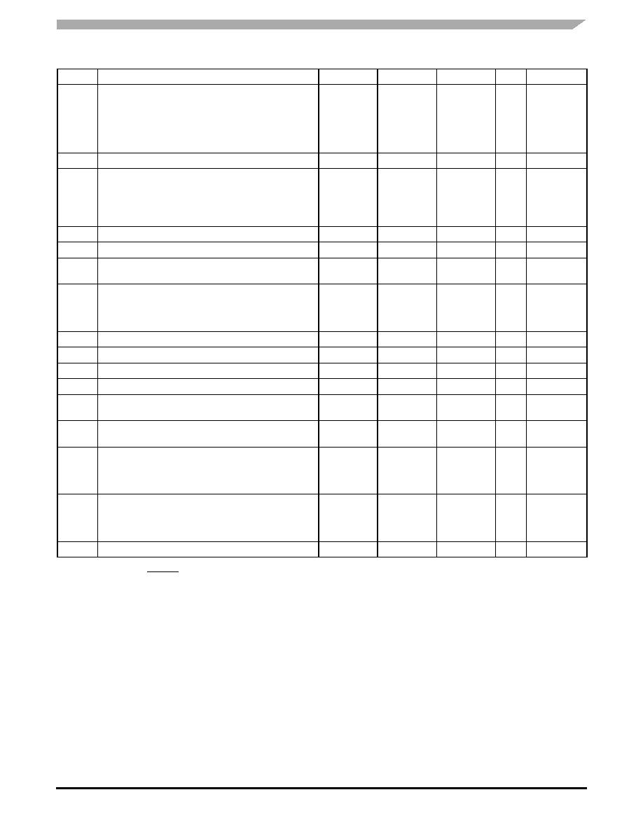
Table 6. AC Characteristics (VCC = 3.3 V ± 5%, TA = 0° to 70°C)(1)
1. AC characteristics apply for parallel output termination of 50
to VTT.
Symbol
Characteristics
Min
Typ
Max
Unit
Condition
fref
Input reference frequency
÷4 feedback
in PLL mode(2) (3)
÷6 feedback
÷8 feedback
÷12 feedback
Input reference frequency in PLL bypass mode(4)
2. PLL mode requires PLL_EN=0 to enable the PLL and zero-delay operation.
3. The PLL may be unstable with a divide by 2 feedback ratio.
4. In PLL bypass mode, the MPC93H52 divides the input reference clock.
50.0
33.3
25.0
16.67
50.0
120.0
80.0
60.0
40.0
250.0
MHz
fVCO
VCO lock frequency range(5)
5. The input frequency fref on CCLK must match the VCO frequency range divided by the feedback divider ratio FB: fref = fVCO ÷ FB.
200
480
MHz
fMAX
Output Frequency
÷2 output(6)
÷4 output
÷6 output
÷8 output
÷12 output
100
50
33.3
25
16.67
240
120
80
60
40
MHz
tPWMIN Minimum Reference Input Pulse Width
2.0
ns
tr, tf
CCLK Input Rise/Fall Time(7)
7. The MPC93H52 will operate with input rise and fall times up to 3.0 ns, but the AC characteristics, specifically t(), can only be guaranteed if
tr/tf are within the specified range.
1.0
ns
0.8 to 2.0 V
t()
Propagation Delay CCLK to FB_IN
(fref = 50 MHz)
(static phase offset)
–200
+200
ps
PLL locked
tsk(O)
Output-to-output Skew(8)
all outputs, any frequency
within QA output bank
within QB output bank
within QC output bank
8. See application section for part-to-part skew calculation.
300
200
100
ps
DC
Output duty cycle
45
50
55
%
tr, tf
Output Rise/Fall Time
0.1
1.0
ns
0.55 to 2.4 V
tPLZ, HZ Output Disable Time
8
ns
tPZL, LZ Output Enable Time
10
ns
tJIT(CC) Cycle-to-cycle jitter
output frequencies mixed
all outputs same frequency
150
25
ps
RMS
tJIT(PER) Period Jitter
output frequencies mixed
all outputs same frequency
75
20
ps
RMS
tJIT()
I/O Phase Jitter(9)
÷4 feedback divider RMS (1 σ)
÷6 feedback divider RMS (1 σ)
÷8 feedback divider RMS (1 σ)
÷12 feedback divider RMS (1 σ)
9. See application section for a jitter calculation for other confidence factors than 1
σ.
40
ps
BW
PLL closed loop bandwidth(10)
÷4 feedback
÷6 feedback
÷8 feedback
÷12 feedback
10. –3 dB point of PLL transfer characteristics.
2.0–8.0
1.0–4.0
0.8–2.5
0.6–1.5
MHz
tLOCK
Maximum PLL Lock Time
10
ms
相关PDF资料 |
PDF描述 |
|---|---|
| MPC93R51FAR2 | 93R SERIES, PLL BASED CLOCK DRIVER, 9 TRUE OUTPUT(S), 0 INVERTED OUTPUT(S), PQFP32 |
| MPC93R51FA | 93R SERIES, PLL BASED CLOCK DRIVER, 9 TRUE OUTPUT(S), 0 INVERTED OUTPUT(S), PQFP32 |
| MPC93R51ACR2 | 93R SERIES, PLL BASED CLOCK DRIVER, 9 TRUE OUTPUT(S), 0 INVERTED OUTPUT(S), PQFP32 |
| MPC940LFAR2 | MPC900 SERIES, LOW SKEW CLOCK DRIVER, 18 TRUE OUTPUT(S), 0 INVERTED OUTPUT(S), PQFP32 |
| MPC940LFA | MPC900 SERIES, LOW SKEW CLOCK DRIVER, 18 TRUE OUTPUT(S), 0 INVERTED OUTPUT(S), PQFP32 |
相关代理商/技术参数 |
参数描述 |
|---|---|
| MPC93H52FA | 功能描述:IC CLOCK GEN/DVR HI-DRIVE 32LQFP RoHS:否 类别:集成电路 (IC) >> 时钟/计时 - 时钟发生器,PLL,频率合成器 系列:- 标准包装:39 系列:- 类型:* PLL:带旁路 输入:时钟 输出:时钟 电路数:1 比率 - 输入:输出:1:10 差分 - 输入:输出:是/是 频率 - 最大:170MHz 除法器/乘法器:无/无 电源电压:2.375 V ~ 3.465 V 工作温度:0°C ~ 70°C 安装类型:* 封装/外壳:* 供应商设备封装:* 包装:* |
| MPC93H52FAR2 | 制造商:Integrated Device Technology Inc 功能描述:ZERO DLY PLL CLOCK GEN SGL 32LQFP - Tape and Reel |
| MPC93R51 | 制造商:MOTOROLA 制造商全称:Motorola, Inc 功能描述:LOW VOLTAGE PLL CLOCK DRIVER |
| MPC93R51AC | 功能描述:时钟驱动器及分配 3.3V 240MHz Clock Generator RoHS:否 制造商:Micrel 乘法/除法因子:1:4 输出类型:Differential 最大输出频率:4.2 GHz 电源电压-最大: 电源电压-最小:5 V 最大工作温度:+ 85 C 封装 / 箱体:SOIC-8 封装:Reel |
| MPC93R51ACR2 | 功能描述:时钟发生器及支持产品 FSL 1-9 LVCMOS/LVPEC L to LVCMOS PLL Cloc RoHS:否 制造商:Silicon Labs 类型:Clock Generators 最大输入频率:14.318 MHz 最大输出频率:166 MHz 输出端数量:16 占空比 - 最大:55 % 工作电源电压:3.3 V 工作电源电流:1 mA 最大工作温度:+ 85 C 安装风格:SMD/SMT 封装 / 箱体:QFN-56 |
发布紧急采购,3分钟左右您将得到回复。