- 您现在的位置:买卖IC网 > PDF目录29137 > MPC93R51ACR2 (FREESCALE SEMICONDUCTOR INC) 93R SERIES, PLL BASED CLOCK DRIVER, 9 TRUE OUTPUT(S), 0 INVERTED OUTPUT(S), PQFP32 PDF资料下载
参数资料
| 型号: | MPC93R51ACR2 |
| 厂商: | FREESCALE SEMICONDUCTOR INC |
| 元件分类: | 时钟及定时 |
| 英文描述: | 93R SERIES, PLL BASED CLOCK DRIVER, 9 TRUE OUTPUT(S), 0 INVERTED OUTPUT(S), PQFP32 |
| 封装: | 7 X 7 MM, LEAD FREE, LQFP-32 |
| 文件页数: | 10/12页 |
| 文件大小: | 339K |
| 代理商: | MPC93R51ACR2 |
Advanced Clock Drivers Devices
Freescale Semiconductor
7
MPC93R51
Calculation of Part-to-Part Skew
The MPC93R51 zero delay buffer supports applications
where critical clock signal timing can be maintained across
several devices. If the reference clock inputs (TCLK or PCLK)
of two or more MPC93R51 are connected together, the
maximum overall timing uncertainty from the common TCLK
input to any output is:
tSK(PP) = t() + tSK(O) + tPD, LINE(FB) + tJIT() CF
This maximum timing uncertainty consists of 4
components: static phase offset, output skew, feedback
board trace delay and I/O (phase) jitter.
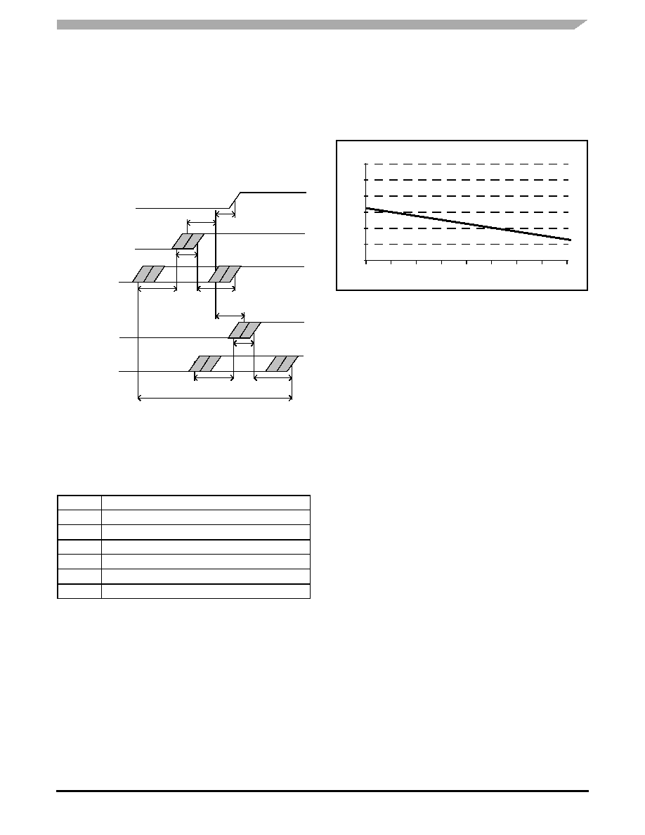
Figure 4. MPC93R51 Max. Device-to-Device Skew
Due to the statistical nature of I/O jitter, a RMS value (1
σ)
is specified. I/O jitter numbers for other confidence factors
(CF) can be derived from Table 8.
The feedback trace delay is determined by the board
layout and can be used to fine-tune the effective delay
through each device. In the following example calculation,
an I/O jitter confidence factor of 99.7% (
± 3σ) is assumed,
resulting in a worst case timing uncertainty from input to any
output of –251 ps to 351 ps relative to TCLK (VCC = 3.3 V and
fVCO = 400 MHz):
tSK(PP) = [-50ps...150ps] + [-150ps...150ps] +
[(17ps –3)...(17ps 3)] + tPD, LINE(FB)
tSK(PP) = [-251ps...351ps] + tPD, LINE(FB)
Above equation uses the maximum I/O jitter number
shown in the AC characteristic table for VCC = 3.3 V (17 ps
RMS). I/O jitter is frequency dependent with a maximum at
the lowest VCO frequency (200 MHz for the MPC93R51).
Applications using a higher VCO frequency exhibit less I/O
jitter than the AC characteristic limit. The I/O jitter
characteristics in Figure 5 can be used to derive a smaller
I/O jitter number at the specific VCO frequency, resulting in
tighter timing limits in zero-delay mode and for part-to-part
skew tSK(PP).
Figure 5. Max. I/O Jitter (RMS) Versus Frequency
for VCC = 3.3 V
Power Supply Filtering
The MPC93R51 is a mixed analog/digital product. Its
analog circuitry is naturally susceptible to random noise,
especially if this noise is seen on the power supply pins.
Noise on the VCCA (PLL) power supply impacts the device
characteristics, for instance, I/O jitter. The MPC93R51
provides separate power supplies for the output buffers (VCC)
and the phase-locked loop (VCCA) of the device. The purpose
of this design technique is to isolate the high switching noise
digital outputs from the relatively sensitive internal analog
phase-locked loop. In a digital system environment where it
is more difficult to minimize noise on the power supplies, a
second level of isolation may be required. The simple but
effective form of isolation is a power supply filter on the VCCA
pin for the MPC93R51.
Figure 6 illustrates a typical power supply filter scheme.
The MPC93R51 frequency and phase stability is most
susceptible to noise with spectral content in the 100 kHz to 20
MHz range; therefore, the filter should be designed to target
this range. The key parameter that needs to be met in the
final filter design is the DC voltage drop across the series filter
resistor RF. From the data sheet, the ICCA current (the current
sourced through the VCCA pin) is typically 3 mA (5 mA
maximum), assuming that a minimum of 3.0 V must be
maintained on the VCCA pin. The resistor RF shown in
Figure 6 must have a resistance of 5-15
to meet the
voltage drop criteria.
Table 8. Confidence Factor CF
CF
Probability of clock edge within the distribution
± 1σ
0.68268948
± 2σ
0.95449988
± 3σ
0.99730007
± 4σ
0.99993663
± 5σ
0.99999943
± 6σ
0.99999999
tPD,LINE(FB)
tJIT()
+tSK(O)
—t()
+t()
tJIT()
+tSK(O)
tSK(PP)
Max. skew
TCLKCommon
QFBDevice 1
Any QDevice 1
QFBDevice2
Any QDevice 2
30
25
20
15
10
5
0
75
225
250
275
300
325
VCO frequency [MHz]
t JI
T(
)[p
s]
m
s
Max. I/O Jitter versus frequency
350
375
400
相关PDF资料 |
PDF描述 |
|---|---|
| MPC940LFAR2 | MPC900 SERIES, LOW SKEW CLOCK DRIVER, 18 TRUE OUTPUT(S), 0 INVERTED OUTPUT(S), PQFP32 |
| MPC940LFA | MPC900 SERIES, LOW SKEW CLOCK DRIVER, 18 TRUE OUTPUT(S), 0 INVERTED OUTPUT(S), PQFP32 |
| MPC942PFAR2 | 942 SERIES, LOW SKEW CLOCK DRIVER, 18 TRUE OUTPUT(S), 0 INVERTED OUTPUT(S), PQFP32 |
| MPC9443AE | 9443 SERIES, LOW SKEW CLOCK DRIVER, 16 TRUE OUTPUT(S), 0 INVERTED OUTPUT(S), PQFP48 |
| MPC9446FAR2 | 9446 SERIES, LOW SKEW CLOCK DRIVER, 10 TRUE OUTPUT(S), 0 INVERTED OUTPUT(S), PQFP32 |
相关代理商/技术参数 |
参数描述 |
|---|---|
| MPC93R51D | 制造商:MOTOROLA 制造商全称:Motorola, Inc 功能描述:LOW VOLTAGE PLL CLOCK DRIVER |
| MPC93R51FA | 功能描述:时钟驱动器及分配 3.3V 240MHz Clock Generator RoHS:否 制造商:Micrel 乘法/除法因子:1:4 输出类型:Differential 最大输出频率:4.2 GHz 电源电压-最大: 电源电压-最小:5 V 最大工作温度:+ 85 C 封装 / 箱体:SOIC-8 封装:Reel |
| MPC93R51FAR2 | 制造商:Integrated Device Technology Inc 功能描述:PLL CLOCK DRVR SGL 32LQFP - Tape and Reel |
| MPC93R52 | 制造商:MOTOROLA 制造商全称:Motorola, Inc 功能描述:LOW VOLTAGE 3.3V LVCMOS 1:11 CLOCK GENERATOR |
| MPC93R52AC | 功能描述:时钟发生器及支持产品 FSL 1-11 LVCMOS PLL Clock Generator, pwr RoHS:否 制造商:Silicon Labs 类型:Clock Generators 最大输入频率:14.318 MHz 最大输出频率:166 MHz 输出端数量:16 占空比 - 最大:55 % 工作电源电压:3.3 V 工作电源电流:1 mA 最大工作温度:+ 85 C 安装风格:SMD/SMT 封装 / 箱体:QFN-56 |
发布紧急采购,3分钟左右您将得到回复。