- 您现在的位置:买卖IC网 > PDF目录2099 > MPC9446FAR2 (IDT, Integrated Device Technology Inc)IC CLK BUFF DVDR MUX 2:10 32LQFP PDF资料下载
参数资料
| 型号: | MPC9446FAR2 |
| 厂商: | IDT, Integrated Device Technology Inc |
| 文件页数: | 1/12页 |
| 文件大小: | 0K |
| 描述: | IC CLK BUFF DVDR MUX 2:10 32LQFP |
| 标准包装: | 2,000 |
| 类型: | 扇出缓冲器(分配),除法器,多路复用器 |
| 电路数: | 1 |
| 比率 - 输入:输出: | 2:10 |
| 差分 - 输入:输出: | 无/无 |
| 输入: | LVCMOS |
| 输出: | LVCMOS |
| 频率 - 最大: | 250MHz |
| 电源电压: | 2.375 V ~ 3.465 V |
| 工作温度: | -40°C ~ 85°C |
| 安装类型: | 表面贴装 |
| 封装/外壳: | 32-LQFP |
| 供应商设备封装: | 32-TQFP(7x7) |
| 包装: | 带卷 (TR) |
DATASHEET
3.3V and 2.5V, LVCMOS Clock Fanout Buffer
MPC9446
NRND
MPC9446 REVISION 5 DECEMBER 21, 2012
1
2012 Integrated Device Technology, Inc.
The MPC9446 is a 2.5 V and 3.3 V compatible 1:10 clock distribution buffer designed
for low-voltage mid-range to high-performance telecom, networking and computing
applications. Both 3.3 V, 2.5 V and dual supply voltages are supported for mixed-voltage
applications. The MPC9446 offers 10 low-skew outputs and 2 selectable inputs for clock
redundancy. The outputs are configurable and support 1:1 and 1:2 output to input
frequency ratios. The MPC9446 is specified for the extended temperature range of –40
C
to 85
C.
Features
Configurable 10 outputs LVCMOS clock distribution buffer
Compatible to single, dual and mixed 3.3 V/2.5 V voltage supply
Wide range output clock frequency up to 250 MHz
Designed for mid-range to high-performance telecom, networking
and computer applications
Supports applications requiring clock redundancy
Maximum output skew of 200 ps (150 ps within one bank)
Selectable output configurations per output bank
Tristable outputs
32-lead LQFP package, Pb-free
Ambient operating temperature range of –40 to 85
C
Functional Description
The MPC9446 is a full static fanout buffer design supporting clock frequencies up to 250
MHz. The signals are generated and retimed on-chip to ensure minimal skew between the
three output banks. Two independent LVCMOS compatible clock inputs are available. This
feature supports redundant clock sources or the addition of a test clock into the system design. Each of the three output banks can be
individually supplied by 2.5 V or 3.3 V supporting mixed voltage applications. The FSELx pins choose between division of the input refer-
ence frequency by one or two. The frequency divider can be set individually for each of the three output banks. The MPC9446 can be
rese,t and the outputs are disabled by deasserting the MR/OE pin (logic high state). Asserting MR/OE will enable the outputs.
All inputs accept LVCMOS signals while the outputs provide LVCMOS compatible levels with the capability to drive terminated 50
transmission lines. Please consult the MPC9456 specification for a 1:10 mixed voltage buffer with LVPECL compatible inputs. For series
terminated transmission lines, each of the MPC9446 outputs can drive one or two traces giving the devices an effective fanout of 1:20.
The device is packaged in a 7x7 mm2 32-lead LQFP package.
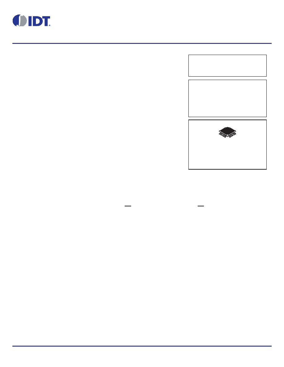
AC SUFFIX
32-LEAD LQFP PACKAGE
Pb-FREE PACKAGE
CASE 873A-04
MPC9446
LOW VOLTAGE SINGLE OR
DUAL SUPPLY 2.5 V AND 3.3 V
LVCMOS CLOCK
DISTRIBUTION BUFFER
NRND – Not Recommend for New Designs
相关PDF资料 |
PDF描述 |
|---|---|
| MPC9447ACR2 | IC CLOCK BUFFER MUX 2:9 32-LQFP |
| MPC9448ACR2 | IC CLOCK BUFFER MUX 1:12 32-LQFP |
| MPC9449AER2 | IC CLK BUFF DVDR MUX 3:15 52LQFP |
| MPC94551EFR2 | IC CLOCK BUFFER 1:4 160MHZ 8SOIC |
| MPC9456AC | IC CLK BUFF DVDR MUX 1:10 32LQFP |
相关代理商/技术参数 |
参数描述 |
|---|---|
| MPC9447 | 制造商:IDT 制造商全称:Integrated Device Technology 功能描述:3.3V/2.5V 1:9 LVCMOS Clock Fanout Buffer |
| MPC9447AC | 功能描述:时钟缓冲器 2.5 3.3V 250MHz Clock Generator RoHS:否 制造商:Texas Instruments 输出端数量:5 最大输入频率:40 MHz 传播延迟(最大值): 电源电压-最大:3.45 V 电源电压-最小:2.375 V 最大功率耗散: 最大工作温度:+ 85 C 最小工作温度:- 40 C 封装 / 箱体:LLP-24 封装:Reel |
| MPC9447ACR2 | 功能描述:时钟缓冲器 FSL 1-9 LVCMOS Fanout Buffer RoHS:否 制造商:Texas Instruments 输出端数量:5 最大输入频率:40 MHz 传播延迟(最大值): 电源电压-最大:3.45 V 电源电压-最小:2.375 V 最大功率耗散: 最大工作温度:+ 85 C 最小工作温度:- 40 C 封装 / 箱体:LLP-24 封装:Reel |
| MPC9447D | 制造商:MOTOROLA 制造商全称:Motorola, Inc 功能描述:3.3V/2.5V 1:9 LVCMOS Clock Fanout Buffer |
| MPC9447FA | 功能描述:时钟缓冲器 2.5 3.3V 275MHz Clock Generator RoHS:否 制造商:Texas Instruments 输出端数量:5 最大输入频率:40 MHz 传播延迟(最大值): 电源电压-最大:3.45 V 电源电压-最小:2.375 V 最大功率耗散: 最大工作温度:+ 85 C 最小工作温度:- 40 C 封装 / 箱体:LLP-24 封装:Reel |
发布紧急采购,3分钟左右您将得到回复。