- 您现在的位置:买卖IC网 > PDF目录29137 > MPC954DT (MOTOROLA INC) MPC900 SERIES, PLL BASED CLOCK DRIVER, 10 TRUE OUTPUT(S), 0 INVERTED OUTPUT(S), PDSO24 PDF资料下载
参数资料
| 型号: | MPC954DT |
| 厂商: | MOTOROLA INC |
| 元件分类: | 时钟及定时 |
| 英文描述: | MPC900 SERIES, PLL BASED CLOCK DRIVER, 10 TRUE OUTPUT(S), 0 INVERTED OUTPUT(S), PDSO24 |
| 封装: | TSSOP-24 |
| 文件页数: | 4/5页 |
| 文件大小: | 117K |
| 代理商: | MPC954DT |
5
MPC954
MOTOROLA ADVANCED CLOCK DRIVERS DEVICE DATA
460
Power Supply Filtering
The MPC954 is a mixed analog/digital product and as such
it exhibits some sensitivities that would not necessarily be
seen on a fully digital product. Analog circuitry is naturally sus-
ceptible to random noise, especially if this noise is seen on the
power supply pins. The MPC954 provides separate power
supplies for the output buffers (VCCO) and the phase–locked
loop (VCCA) of the device. The purpose of this design tech-
nique is to try and isolate the high switching noise digital out-
puts from the relatively sensitive internal analog phase–locked
loop. In a controlled environment such as an evaluation board
this level of isolation is sufficient. However, in a digital system
environment where it is more difficult to minimize noise on the
power supplies a second level of isolation may be required.
The simplest form of isolation is a power supply filter on the
VCCA pin for the MPC954.
Figure 3 illustrates a typical power supply filter scheme. The
MPC954 is most susceptible to noise with spectral content in
the 1KHz to 10MHz range. Therefore the filter should be de-
signed to target this range. The key parameter that needs to be
met in the final filter design is the DC voltage drop that will be
seen between the VCC supply and the VCCA pin of the
MPC954. From the data sheet the IVCCA current (the current
sourced through the VCCA pin) is typically 15mA (20mA maxi-
mum), assuming that a minimum of 3.0V must be maintained
on the VCCA pin very little DC voltage drop can be tolerated
when a 3.3V VCC supply is used. The resistor shown in
Figure 3 must have a resistance of 10–15
to meet the voltage
drop criteria. The RC filter pictured will provide a broadband
filter with approximately 100:1 attenuation for noise whose
spectral content is above 20KHz. As the noise frequency
crosses the series resonant point of an individual capacitor it’s
overall impedance begins to look inductive and thus increases
with increasing frequency. The parallel capacitor combination
shown ensures that a low impedance path to ground exists for
frequencies well above the bandwidth of the PLL. It is recom-
mended that the user start with an 8–10
resistor to avoid
potential VCC drop problems and only move to the higher value
resistors when a higher level of attenuation is shown to be
needed.
Figure 3. Power Supply Filter
VCCA
VCC
MPC954
0.01F
22F
0.01F
3.3V
RS=5-15
Although the MPC954 has several design features to mini-
mize the susceptibility to power supply noise (isolated power
and grounds and fully differential PLL) there still may be ap-
plications in which overall performance is being degraded due
to system power supply noise. The power supply filter
schemes discussed in this section should be adequate to elim-
inate power supply noise related problems in most designs.
Driving Transmission Lines
The MPC954 clock driver was designed to drive high speed
signals in a terminated transmission line environment. To pro-
vide the optimum flexibility to the user the output drivers were
designed to exhibit the lowest impedance possible. With an
output impedance of approximately 10
the drivers can drive
either parallel or series terminated transmission lines. For
more information on transmission lines the reader is referred to
application note AN1091 in the Timing Solutions data book
(DL207/D).
In most high performance clock networks point–to–point
distribution of signals is the method of choice. In a point–to–
point scheme either series terminated or parallel terminated
transmission lines can be used. The parallel technique termi-
nates the signal at the end of the line with a 50
resistance to
VCC/2. This technique draws a fairly high level of DC current
and thus only a single terminated line can be driven by each
output of the MPC954 clock driver. For the series terminated
case however there is no DC current draw, thus the outputs
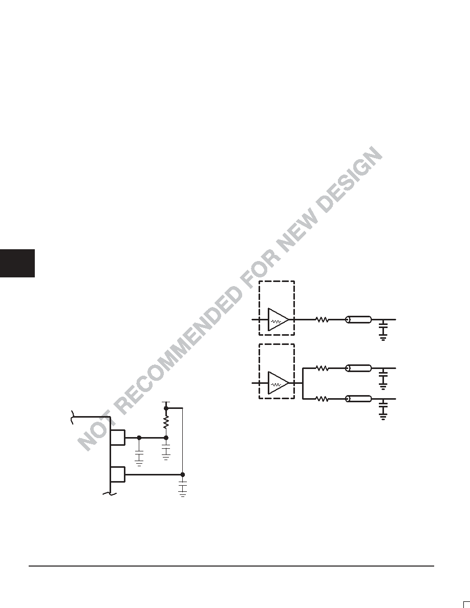
can drive multiple series terminated lines. Figure 4 illustrates
an output driving a single series terminated line vs two series
terminated lines in parallel. When taken to its extreme the fan-
out of the MPC954 clock driver is effectively doubled due to its
capability to drive multiple lines.
Figure 4. Single versus Dual Transmission Lines
7
IN
MPC954
OUTPUT
BUFFER
RS = 43
ZO = 50
OutA
7
IN
MPC954
OUTPUT
BUFFER
RS = 36
ZO = 50
OutB0
RS = 36
ZO = 50
OutB1
The waveform plots of Figure 5 show the simulation results
of an output driving a single line vs two lines. In both cases the
drive capability of the MPC954 output buffers is more than suf-
ficient to drive 50
transmission lines on the incident edge.
Note from the delay measurements in the simulations a delta
of only 43ps exists between the two differently loaded outputs.
This suggests that the dual line driving need not be used exclu-
sively to maintain the tight output–to–output skew of the
MPC954. The output waveform in Figure 5 shows a step in the
waveform, this step is caused by the impedance mismatch
seen looking into the driver. The parallel combination of the
43
series resistor plus the output impedance does not match
the parallel combination of the line impedances. The voltage
wave launched down the two lines will equal:
相关PDF资料 |
PDF描述 |
|---|---|
| MPC961PFA | 961 SERIES, PLL BASED CLOCK DRIVER, 17 TRUE OUTPUT(S), 0 INVERTED OUTPUT(S), PQFP32 |
| MPC962308D-4R2 | 962308 SERIES, PLL BASED CLOCK DRIVER, 8 TRUE OUTPUT(S), 0 INVERTED OUTPUT(S), PDSO16 |
| MPC962308D-2 | 962308 SERIES, PLL BASED CLOCK DRIVER, 8 TRUE OUTPUT(S), 0 INVERTED OUTPUT(S), PDSO16 |
| MPC962308D-5H | 962308 SERIES, PLL BASED CLOCK DRIVER, 8 TRUE OUTPUT(S), 0 INVERTED OUTPUT(S), PDSO16 |
| MPC962308D-3 | 962308 SERIES, PLL BASED CLOCK DRIVER, 8 TRUE OUTPUT(S), 0 INVERTED OUTPUT(S), PDSO16 |
相关代理商/技术参数 |
参数描述 |
|---|---|
| MPC958 | 制造商:MOTOROLA 制造商全称:Motorola, Inc 功能描述:LOW VOLTAGE PLL CLOCK DRIVER |
| MPC9600 | 制造商:MOTOROLA 制造商全称:Motorola, Inc 功能描述:LOW VOLTAGE 2.5 V AND 3.3 V CMOS PLL CLOCK DRIVER |
| MPC9600AE | 功能描述:时钟发生器及支持产品 RoHS:否 制造商:Silicon Labs 类型:Clock Generators 最大输入频率:14.318 MHz 最大输出频率:166 MHz 输出端数量:16 占空比 - 最大:55 % 工作电源电压:3.3 V 工作电源电流:1 mA 最大工作温度:+ 85 C 安装风格:SMD/SMT 封装 / 箱体:QFN-56 |
| MPC9600AER2 | 功能描述:时钟缓冲器 RoHS:否 制造商:Texas Instruments 输出端数量:5 最大输入频率:40 MHz 传播延迟(最大值): 电源电压-最大:3.45 V 电源电压-最小:2.375 V 最大功率耗散: 最大工作温度:+ 85 C 最小工作温度:- 40 C 封装 / 箱体:LLP-24 封装:Reel |
| MPC9600FA | 功能描述:IC CLOCK DRVR PLL LV 1:21 48LQFP RoHS:否 类别:集成电路 (IC) >> 时钟/计时 - 时钟发生器,PLL,频率合成器 系列:- 标准包装:39 系列:- 类型:* PLL:带旁路 输入:时钟 输出:时钟 电路数:1 比率 - 输入:输出:1:10 差分 - 输入:输出:是/是 频率 - 最大:170MHz 除法器/乘法器:无/无 电源电压:2.375 V ~ 3.465 V 工作温度:0°C ~ 70°C 安装类型:* 封装/外壳:* 供应商设备封装:* 包装:* |
发布紧急采购,3分钟左右您将得到回复。