- 您现在的位置:买卖IC网 > PDF目录29137 > MPC962308D-2R2 (INTEGRATED DEVICE TECHNOLOGY INC) 962308 SERIES, PLL BASED CLOCK DRIVER, 8 TRUE OUTPUT(S), 0 INVERTED OUTPUT(S), PDSO16 PDF资料下载
参数资料
| 型号: | MPC962308D-2R2 |
| 厂商: | INTEGRATED DEVICE TECHNOLOGY INC |
| 元件分类: | 时钟及定时 |
| 英文描述: | 962308 SERIES, PLL BASED CLOCK DRIVER, 8 TRUE OUTPUT(S), 0 INVERTED OUTPUT(S), PDSO16 |
| 封装: | 0.150 INCH, SOIC-16 |
| 文件页数: | 1/8页 |
| 文件大小: | 299K |
| 代理商: | MPC962308D-2R2 |
FREESCALE SEMICONDUCTOR ADVANCED CLOCK DRIVERS DEVICE DATA
513
Freescale Semiconductor, Inc.
TECHNICAL DATA
Order number: MPC962308
Rev 3, 08/2004
3.3 V Zero Delay Buffer
The MPC962308 is a 3.3 V Zero Delay Buffer designed to distribute
high-speed clocks in PC, workstation, datacom, telecom and other
high-performance applications. The MPC962308 uses an internal PLL and an
external feedback path to lock its low-skew clock output phase to the reference
clock phase, providing virtually zero propagation delay. The input-to-output
skew is guaranteed to be less than 250 ps and output-to-output skew is
guaranteed to be less than 200 ps.
Features
1:8 outputs LVCMOS zero-delay buffer
Zero input-output propagation delay, adjustable by the capacitive load on
FBK input
Multiple Configurations, see Table 11. Available MPC962308
Configurations
Multiple low-skew outputs
200 ps max output-output skew
700 ps max device-device skew
Two banks of four outputs, output tristate control by two select inputs
Supports a clock I/O frequency range of 10 MHz to 133 MHz
Low jitter, 200 ps max cycle-cycle (-1, -1H, -4, -5H)
±250 ps static phase offset (SPO)
16-pin SOIC package or 16-pin TSSOP package
Single 3.3 V supply
Ambient temperature range: –40
°C to +85°C
Compatible with the CY2308 and CY23S08
Spread spectrum compatible
Functional Description
The MPC962308 has two banks of four outputs each which can be controlled by the select inputs as shown in Table 10. Select
Input Decoding. Bank B can be tristated if all of the outputs are not required. The select inputs also allow the input clock to be directly
applied to the output for chip and system testing purposes. The MPC962308 PLL enters a power down state when there are no rising
edges on the REF input. During this state, all of the outputs are in tristate and there is less than 50
A of current draw. The PLL shuts
down in two additional cases explained in Table 10. Select Input Decoding.
Multiple MPC962308 devices can accept and distribute the same input clock throughout the system. In this situation, the difference
between the output skews of two devices will be less than 700 ps.
The MPC962308 is available in five different configurations as shown in Table 11. Available MPC962308 Configurations. In the
MPC962308-1, the reference frequency is reproduced by the PLL and provided at the outputs. A high drive version of this configura-
tion, the MPC962308-1H, is available to provide faster rise and fall times of the device.
The MPC962308-2 provides 2X and 1X the reference frequency at the output banks. In addition, the MPC962308-3 provides 4X
and 2X the reference frequency at the output banks. The output banks driving the feedback will determine the different configurations
of the above devices. The MPC962308-4 provides outputs 2X the reference frequency.The MPC962308-5H is a high drive version
with outputs of REF/2.
The MPC962308 is fully 3.3 V compatible and requires no external components for the internal PLL. All inputs accept LVCMOS
signals while the outputs provide LVCMOS compatible levels with the capability to drive terminated 50
transmission lines on the
incident edge. Depending on the configuration, the device is offered in a 16-lead SOIC or 16-lead TSSOP package.
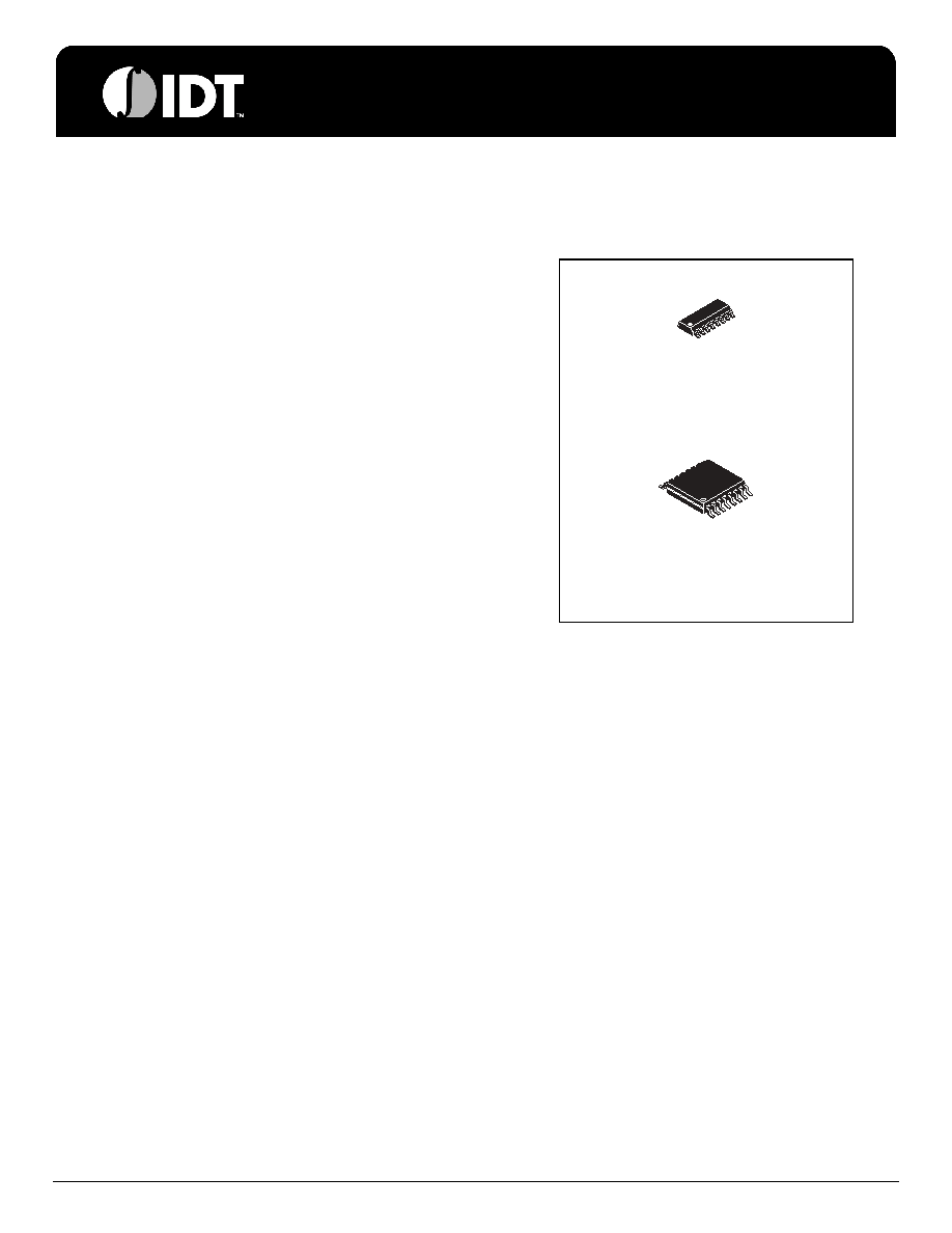
MPC962308
DT SUFFIX
16-LEAD TSSOP PACKAGE
CASE 948F-01
D SUFFIX
16-LEAD SOIC PACKAGE
CASE 751B-05
DATA SHEET
MPC962308
IDT 3.3 V Zero Delay Buffer
Freescale Timing Solutions Organization has been acquired by Integrated Device Technology, Inc
MPC962308
1
3.3 V Zero Delay Buffer
相关PDF资料 |
PDF描述 |
|---|---|
| MPC9653FA | PLL BASED CLOCK DRIVER, 8 TRUE OUTPUT(S), 0 INVERTED OUTPUT(S), PQFP32 |
| MPC9658ACR2 | 9658 SERIES, PLL BASED CLOCK DRIVER, 10 TRUE OUTPUT(S), 0 INVERTED OUTPUT(S), PQFP32 |
| MPC9658FA | 9658 SERIES, PLL BASED CLOCK DRIVER, 10 TRUE OUTPUT(S), 0 INVERTED OUTPUT(S), PQFP32 |
| MPC9658ACR2 | 9658 SERIES, PLL BASED CLOCK DRIVER, 10 TRUE OUTPUT(S), 0 INVERTED OUTPUT(S), PQFP32 |
| MPC973FA | 973 SERIES, PLL BASED CLOCK DRIVER, 12 TRUE OUTPUT(S), 0 INVERTED OUTPUT(S), PQFP52 |
相关代理商/技术参数 |
参数描述 |
|---|---|
| MPC962308D-3 | 制造商:MOTOROLA 制造商全称:Motorola, Inc 功能描述:3.3 V Zero Delay Buffer |
| MPC962308D-3R2 | 制造商:MOTOROLA 制造商全称:Motorola, Inc 功能描述:3.3 V Zero Delay Buffer |
| MPC962308D-4 | 制造商:MOTOROLA 制造商全称:Motorola, Inc 功能描述:3.3 V Zero Delay Buffer |
| MPC962308D-4R2 | 制造商:MOTOROLA 制造商全称:Motorola, Inc 功能描述:3.3 V Zero Delay Buffer |
| MPC962308D-5H | 制造商:MOTOROLA 制造商全称:Motorola, Inc 功能描述:3.3 V Zero Delay Buffer |
发布紧急采购,3分钟左右您将得到回复。