- 您现在的位置:买卖IC网 > PDF目录29137 > MPC9658ACR2 (INTEGRATED DEVICE TECHNOLOGY INC) 9658 SERIES, PLL BASED CLOCK DRIVER, 10 TRUE OUTPUT(S), 0 INVERTED OUTPUT(S), PQFP32 PDF资料下载
参数资料
| 型号: | MPC9658ACR2 |
| 厂商: | INTEGRATED DEVICE TECHNOLOGY INC |
| 元件分类: | 时钟及定时 |
| 英文描述: | 9658 SERIES, PLL BASED CLOCK DRIVER, 10 TRUE OUTPUT(S), 0 INVERTED OUTPUT(S), PQFP32 |
| 封装: | 7 X 7 MM, LEAD FREE, LQFP-32 |
| 文件页数: | 1/12页 |
| 文件大小: | 344K |
| 代理商: | MPC9658ACR2 |
MPC9658
Rev 5, 10/2004
Freescale Semiconductor
Technical Data
Freescale Semiconductor, Inc., 2004. All rights reserved.
3.3 V 1:10 LVCMOS PLL Clock
Generator
The MPC9658 is a 3.3 V compatible, 1:10 PLL based clock generator and
zero-delay buffer targeted for high performance low-skew clock distribution in
mid-range to high-performance telecom, networking and computing applications.
With output frequencies up to 250 MHz and output skews less than 120 ps the
device meets the needs of the most demanding clock applications. The
MPC9658 is specified for the temperature range of 0°C to +70°C.
Features
1:10 PLL based low-voltage clock generator
Supports zero-delay operation
3.3 V power supply
Generates clock signals up to 250 MHz
Maximum output skew of 120 ps
Differential LVPECL reference clock input
External PLL feedback
Drives up to 20 clock lines
32-lead LQFP packaging
32-lead Pb-free Package Available
Pin and function compatible to the MPC958
Functional Description
The MPC9658 utilizes PLL technology to frequency lock its outputs onto an
input reference clock. Normal operation of the MPC9658 requires the connection
of the QFB output to the feedback input to close the PLL feedback path (external
feedback). With the PLL locked, the output frequency is equal to the reference frequency of the device and VCO_SEL selects
the operating frequency range of 50 to 125 MHz or 100 to 250 MHz. The two available post-PLL dividers selected by VCO_SEL
(divide-by-2 or divide-by-4) and the reference clock frequency determine the VCO frequency. Both must be selected to match the
VCO frequency range. The internal VCO of the MPC9658 is running at either 2x or 4x of the reference clock frequency.
The MPC9658 has a differential LVPECL reference input along with an external feedback input. The MPC9658 is ideal for use
as a zero delay, low skew fanout buffer. The device performance has been tuned and optimized for zero delay performance.
The PLL_EN and BYPASS controls select the PLL bypass configuration for test and diagnosis. In this configuration, the se-
lected input reference clock is bypassing the PLL and routed either to the output dividers or directly to the outputs. The PLL by-
pass configurations are fully static and the minimum clock frequency specification and all other PLL characteristics do not apply.
The outputs can be disabled (high-impedance) and the device reset by asserting the MR/OE pin. Asserting MR/OE also causes
the PLL to loose lock due to missing feedback signal presence at FB_IN. Deasserting MR/OE will enable the outputs and close
the phase locked loop, enabling the PLL to recover to normal operation.
The MPC9658 is fully 3.3 V compatible and requires no external loop filter components. The inputs (except PCLK) accept
LVCMOS except signals while the outputs provide LVCMOS compatible levels with the capability to drive terminated 50
trans-
mission lines. For series terminated transmission lines, each of the MPC9658 outputs can drive one or two traces giving the de-
vices an effective fanout of 1:16. The device is packaged in a 7x7 mm2 32-lead LQFP package.
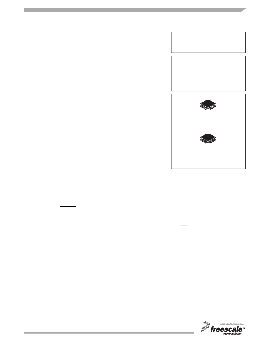
MPC9658
LOW VOLTAGE
3.3 V LVCMOS 1:10
PLL CLOCK GENERATOR
FA SUFFIX
32-LEAD LQFP PACKAGE
CASE 873A-03
AC SUFFIX
32-LEAD LQFP PACKAGE
Pb-FREE PACKAGE
CASE 873A-03
相关PDF资料 |
PDF描述 |
|---|---|
| MPC973FA | 973 SERIES, PLL BASED CLOCK DRIVER, 12 TRUE OUTPUT(S), 0 INVERTED OUTPUT(S), PQFP52 |
| MPC974FAR2 | 974 SERIES, PLL BASED CLOCK DRIVER, 14 TRUE OUTPUT(S), 0 INVERTED OUTPUT(S), PQFP52 |
| MPC974FA | 974 SERIES, PLL BASED CLOCK DRIVER, 14 TRUE OUTPUT(S), 0 INVERTED OUTPUT(S), PQFP52 |
| MPC974FA | 974 SERIES, PLL BASED CLOCK DRIVER, 14 TRUE OUTPUT(S), 0 INVERTED OUTPUT(S), PQFP52 |
| MPC9773AE | 9773 SERIES, PLL BASED CLOCK DRIVER, 12 TRUE OUTPUT(S), 0 INVERTED OUTPUT(S), PQFP52 |
相关代理商/技术参数 |
参数描述 |
|---|---|
| MPC9658FA | 功能描述:时钟发生器及支持产品 2.5 3.3V 250MHz Clock Generator RoHS:否 制造商:Silicon Labs 类型:Clock Generators 最大输入频率:14.318 MHz 最大输出频率:166 MHz 输出端数量:16 占空比 - 最大:55 % 工作电源电压:3.3 V 工作电源电流:1 mA 最大工作温度:+ 85 C 安装风格:SMD/SMT 封装 / 箱体:QFN-56 |
| MPC9658FAR2 | 制造商:Integrated Device Technology Inc 功能描述:PLL Clock Driver Single 32-Pin LQFP T/R 制造商:Integrated Device Technology Inc 功能描述:MPC9658FAR2 - Tape and Reel |
| MPC96877VK | 功能描述:时钟发生器及支持产品 DDR2 PLL RoHS:否 制造商:Silicon Labs 类型:Clock Generators 最大输入频率:14.318 MHz 最大输出频率:166 MHz 输出端数量:16 占空比 - 最大:55 % 工作电源电压:3.3 V 工作电源电流:1 mA 最大工作温度:+ 85 C 安装风格:SMD/SMT 封装 / 箱体:QFN-56 |
| MPC96877VKR2 | 功能描述:时钟发生器及支持产品 DDR2 PLL RoHS:否 制造商:Silicon Labs 类型:Clock Generators 最大输入频率:14.318 MHz 最大输出频率:166 MHz 输出端数量:16 占空比 - 最大:55 % 工作电源电压:3.3 V 工作电源电流:1 mA 最大工作温度:+ 85 C 安装风格:SMD/SMT 封装 / 箱体:QFN-56 |
| MPC970 | 制造商:MOTOROLA 制造商全称:Motorola, Inc 功能描述:LOW VOLTAGE PLL CLOCK DRIVER |
发布紧急采购,3分钟左右您将得到回复。