- 您现在的位置:买卖IC网 > PDF目录26839 > MPC96877VKR2 (FREESCALE SEMICONDUCTOR INC) 96877 SERIES, PLL BASED CLOCK DRIVER, 10 TRUE OUTPUT(S), 0 INVERTED OUTPUT(S), PBGA52 PDF资料下载
参数资料
| 型号: | MPC96877VKR2 |
| 厂商: | FREESCALE SEMICONDUCTOR INC |
| 元件分类: | 时钟及定时 |
| 英文描述: | 96877 SERIES, PLL BASED CLOCK DRIVER, 10 TRUE OUTPUT(S), 0 INVERTED OUTPUT(S), PBGA52 |
| 封装: | 4.50 X 7 MM, 0.65 MM PITCH, LEAD FREE, MO-225BA, MAPBGA-52 |
| 文件页数: | 1/16页 |
| 文件大小: | 395K |
| 代理商: | MPC96877VKR2 |
MPC96877
Rev 3, 08/2005
Freescale Semiconductor
Technical Data
Freescale Semiconductor, Inc., 2005. All rights reserved.
1.8 V PLL 1:10 Differential SDRAM
Clock Driver
Recommended Applications
DDR II Memory Modules
Zero Delay Board fan-out
Features
1.8 V Phase Lock Loop Clock Driver for (DDR II) Applications
Spread Spectrum Clock Compatible
Operating Frequency: 100 MHz to 450 MHz
Supports DDR2 400/533 MHz and DDR2 667 MHz Clock Data Rates
1 to 10 Differential Clock Distribution (SSTL_18)
52-Ball VF-BGA (FP-MAPBGA 0.65-mm Pitch) and 40-Pin MLF (QFN)
52-Lead Pb-Free Package Available
External Feedback Pins (FBIN, FBIN) are used to Synchronize the Outputs
to the Input Clocks
Single-Ended Input and Single-Ended Output Modes
Meets or Exceeds JESD82-8 PLL Standard for PC2-3200/4300
Auto Power Down detect logic
Switching Characteristics
Cycle-to-Cycle Jitter (>165 MHz): 40 ps max.
Output-to-Output Skew: 40 ps max.
Functional Description
The MPC96877 is a high-performance, low-jitter, low-skew, zero-delay buffer
that distributes a differential clock input pair (CK, CK) to ten differential pairs of
clock outputs (Yn, Yn) and to one differential pair of feedback clock outputs
(FBOUT, FBOUT). The clock outputs are controlled by the input clocks (CK, CK),
the feedback clocks (FBIN, FBIN), the LVCMOS control pins (OE, OS), and the
analog power input (AVDD). When OE is low, the clock outputs, except FBOUT/
FBOUT, are disabled while the internal PLL continues to maintain its locked-in
frequency. OS (output select) is a program pin that must be tied to GND or VDD.
When OS is high, OE functions as previously described. When OS and OE are both low, OE has no affect on Y7/Y7, they are
free running. When AVDD is grounded, the PLL is turned off and bypassed for test purposes. When both clock inputs (CK, CK)
are logic low, the device enters in a low power mode. An input logic detection circuit on the differential inputs, independent from
input buffers, detects the logic low level and performs in a low power state where all outputs, the feedback, and the PLL are off.
When the clock inputs transition from being logic low to being differential signals, the PLL turns back on, the inputs and the out-
puts are enabled, and the PLL obtains phase lock between the feedback clock pair (FBIN, FBIN) and the clock input pair (CK,
CK) within the specified stabilization time.
The MPC96877 is able to track spread spectrum clocking (SSC) for reduced EMI. This device operates from 0°C to 70°C.
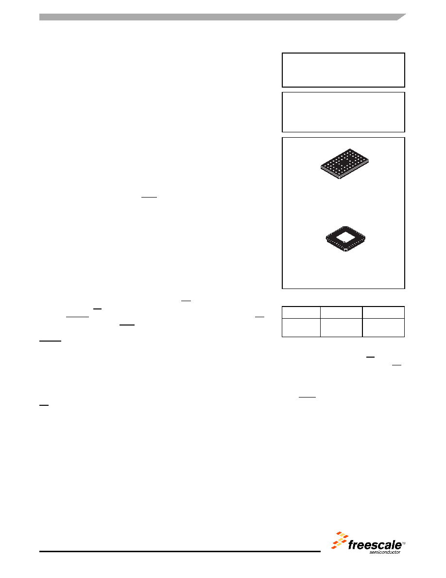
MPC96877
VK SUFFIX
52-BALL FP-MAPBGA PACKAGE
CASE 1544-01
DDR II MEMORY
CLOCK / ZERO DELAY BUFFER
EP SUFFIX
40-PIN MLF/QFN PACKAGE
CASE 1545-01
AVAILABLE ORDERING OPTIONS
TA
52-Ball BGA
40-Pin QFN
0
°C to 70°C MPC96877VK
(Pb-Free)
MPC96877EP
(Pb-Free)
相关PDF资料 |
PDF描述 |
|---|---|
| MPC974FAR2 | 974 SERIES, PLL BASED CLOCK DRIVER, 14 TRUE OUTPUT(S), 0 INVERTED OUTPUT(S), PQFP52 |
| MPC9774FA | 9774 SERIES, PLL BASED CLOCK DRIVER, 14 TRUE OUTPUT(S), 0 INVERTED OUTPUT(S), PQFP52 |
| MPC9774AE | 9774 SERIES, PLL BASED CLOCK DRIVER, 14 TRUE OUTPUT(S), 0 INVERTED OUTPUT(S), PQFP52 |
| MPC97H73FAR2 | PLL BASED CLOCK DRIVER, 13 TRUE OUTPUT(S), 0 INVERTED OUTPUT(S), PQFP52 |
| MPC9893AE | 9893 SERIES, PLL BASED CLOCK DRIVER, 12 TRUE OUTPUT(S), 0 INVERTED OUTPUT(S), PQFP48 |
相关代理商/技术参数 |
参数描述 |
|---|---|
| MPC970 | 制造商:MOTOROLA 制造商全称:Motorola, Inc 功能描述:LOW VOLTAGE PLL CLOCK DRIVER |
| MPC972 | 制造商:Motorola Inc 功能描述: |
| MPC972FA | 制造商:Freescale Semiconductor 功能描述: |
| MPC972H10 F44A WAF | 制造商:Motorola Inc 功能描述: |
| MPC973 | 制造商:MOTOROLA 制造商全称:Motorola, Inc 功能描述:LOW VOLTAGE PLL CLOCK DRIVER |
发布紧急采购,3分钟左右您将得到回复。