- 您现在的位置:买卖IC网 > PDF目录29137 > MPC993FA (INTEGRATED DEVICE TECHNOLOGY INC) 993 SERIES, PLL BASED CLOCK DRIVER, 5 TRUE OUTPUT(S), 0 INVERTED OUTPUT(S), PQFP32 PDF资料下载
参数资料
| 型号: | MPC993FA |
| 厂商: | INTEGRATED DEVICE TECHNOLOGY INC |
| 元件分类: | 时钟及定时 |
| 英文描述: | 993 SERIES, PLL BASED CLOCK DRIVER, 5 TRUE OUTPUT(S), 0 INVERTED OUTPUT(S), PQFP32 |
| 封装: | PLASTIC, LQFP-32 |
| 文件页数: | 3/6页 |
| 文件大小: | 298K |
| 代理商: | MPC993FA |
MPC993
TIMING SOLUTIONS
DL207 — Rev 0
3
MOTOROLA
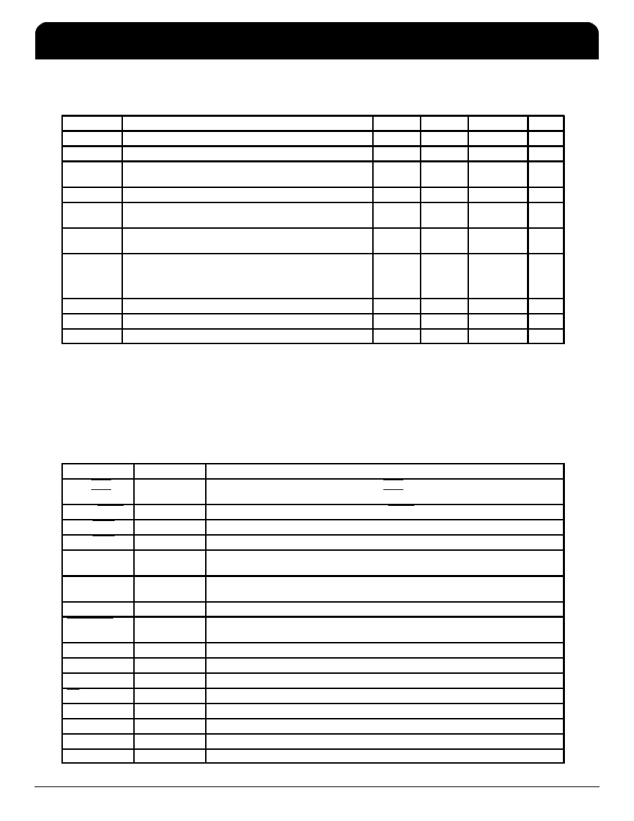
3.3V PECL AC Characteristics (TA = –40°C to 85°C, VCC = 3.3V ± 5%) (Note 6.)
Symbol
Parameter
Min
Typ
Max
Unit
fVCO
PLL VCO Lock Range
(Note 5.)
200
360
MHz
tpwi
25
75
%
tpd
Propagation Delay (Note 1.)
CLKn to Q (Bypass)
CLKn to Ext_FB (Locked (Note 2.))
1.7
–150
2.3
0
2.8
170
ns
ps
tr/tf
Output Rise/Fall Time
200
800
ps
tskew
Output Skew
Within Bank
All Outputs
70
100
ps
pe
Maximum Phase Error Deviation
TBD (Note 3.)
TBD (Note 4.)
ps
per/cycle
Rate of Change of Periods
75MHz Output (Note 1., 3.)
150MHz Output (Note 1., 3.)
75MHz Output (Note 1., 4.)
150MHz Output (Note 1., 4.)
20
10
200
100
50
25
400
200
ps/
cycle
tpw
Output Duty Cycle
45
55
%
tjitter
Cycle–to–Cycle Jitter, Standard Deviation (RMS)
(Note 1.)
20
ps
tlock
Maximum PLL Lock Time
10
ms
1. Guaranteed, not production tested.
2. Static phase offset between the selected reference clock and the feedback signal.
3. Specification holds for a clock switch between two signals no greater than 400ps out of phase. Delta period change per cycle is averaged over
the clock switch excursion. (See Applications Information section on page 4 for more detail)
4. Specification holds for a clock switch between two signals no greater than
±π out of phase. Delta period change per cycle is averaged over the
clock switch excursion.
5. The PLL will be unstable using a
B2 output as the feedback. Either one of the B4 outputs (Qa0 or Qa1) should be used as the feedback signal.
6. PECL output termination is 50 ohms to VCC – 2.0V.
PIN DESCRIPTIONS
Pin Name
I/O
Pin Definition
CLK0, CLK0
CLK1, CLK1
LVPECL Input
Differential PLL clock reference (CLK0 pulldown, CLK0 pullup)
Differential PLL clock reference (CLK1 pulldown, CLK1 pullup)
Ext_FB, Ext_FB
LVPECL Input
Differential PLL feedback clock (Ext_FB pulldown, Ext_FB pullup)
Qa0:1, Qa0:1
LVPECL Output
Differential 1x output pairs
Qb0:2, Qb0:2
LVPECL Output
Differential 2x output pairs
Inp0bad
LVCMOS Output
Indicates detection of a bad input reference clock 0 with respect to the feedback signal. The output
is active HIGH and will remain HIGH until the alarm reset is asserted
Inp1bad
LVCMOS Output
Indicates detection of a bad input reference clock 1 with respect to the feedback signal. The output
is active HIGH and will remain HIGH until the alarm reset is asserted
Clk_Selected
LVCMOS Output
‘0’ if clock 0 is selected, ‘1’ if clock 1 is selected
Alarm_Reset
LVCMOS Input
‘0’ will reset the input bad flags and align Clk_Selected with Sel_Clk. The input is “one–shotted”
(50k
pullup)
Sel_Clk
LVCMOS Input
‘0’ selects CLK0, ‘1’ selects CLK1 (50k
pulldown)
Manual_Override
LVCMOS Input
‘1’ disables internal clock switch circuitry (50k
pulldown)
PLL_En
LVCMOS Input
‘0’ bypasses selected input reference around the phase–locked loop (50k
pullup)
MR
LVCMOS Input
‘0’ resets the internal dividers forcing Q outputs LOW. Asynchronous to the clock (50k
pullup)
VCCA
Power Supply
PLL power supply
VCC
Power Supply
Digital power supply
GNDA
Power Supply
PLL ground
GND
Power Supply
Digital ground
F
re
e
sc
a
le
S
e
m
ic
o
n
d
u
c
to
r,
I
Freescale Semiconductor, Inc.
For More Information On This Product,
Go to: www.freescale.com
n
c
..
.
MPC993
Intelligent Dynamic Clock Switch (IDCS) PLL Clock Driver
NETCOM
IDT Intelligent Dynamic Clock Switch (IDCS) PLL Clock Driver
Freescale Timing Solutions Organization has been acquired by Integrated Device Technology, Inc
MPC993
3
相关PDF资料 |
PDF描述 |
|---|---|
| MPC9952FAR2 | PLL BASED CLOCK DRIVER, 11 TRUE OUTPUT(S), 0 INVERTED OUTPUT(S), PQFP32 |
| MPC9952FA | PLL BASED CLOCK DRIVER, 11 TRUE OUTPUT(S), 0 INVERTED OUTPUT(S), PQFP32 |
| MPC9993ACR2 | 9993 SERIES, PLL BASED CLOCK DRIVER, 5 TRUE OUTPUT(S), 0 INVERTED OUTPUT(S), PQFP32 |
| MPC9993AC | 9993 SERIES, PLL BASED CLOCK DRIVER, 5 TRUE OUTPUT(S), 0 INVERTED OUTPUT(S), PQFP32 |
| MSFLDL-TTL-200 | ACTIVE DELAY LINE, TRUE OUTPUT, SIP4 |
相关代理商/技术参数 |
参数描述 |
|---|---|
| MPC9992 | 制造商:MOTOROLA 制造商全称:Motorola, Inc 功能描述:3.3 DIFFRERENTIAL ECL/PECL PLL CLOCK GENERATOR |
| MPC9992AC | 功能描述:时钟发生器及支持产品 RoHS:否 制造商:Silicon Labs 类型:Clock Generators 最大输入频率:14.318 MHz 最大输出频率:166 MHz 输出端数量:16 占空比 - 最大:55 % 工作电源电压:3.3 V 工作电源电流:1 mA 最大工作温度:+ 85 C 安装风格:SMD/SMT 封装 / 箱体:QFN-56 |
| MPC9992ACR2 | 功能描述:时钟发生器及支持产品 RoHS:否 制造商:Silicon Labs 类型:Clock Generators 最大输入频率:14.318 MHz 最大输出频率:166 MHz 输出端数量:16 占空比 - 最大:55 % 工作电源电压:3.3 V 工作电源电流:1 mA 最大工作温度:+ 85 C 安装风格:SMD/SMT 封装 / 箱体:QFN-56 |
| MPC9992FA | 功能描述:锁相环 - PLL 2.5 3.3V 400MHz Clock Generator RoHS:否 制造商:Silicon Labs 类型:PLL Clock Multiplier 电路数量:1 最大输入频率:710 MHz 最小输入频率:0.002 MHz 输出频率范围:0.002 MHz to 808 MHz 电源电压-最大:3.63 V 电源电压-最小:1.71 V 最大工作温度:+ 85 C 最小工作温度:- 40 C 封装 / 箱体:QFN-36 封装:Tray |
| MPC9992FAR2 | 制造商:Integrated Device Technology Inc 功能描述:PLL Clock Driver Single 32-Pin LQFP T/R |
发布紧急采购,3分钟左右您将得到回复。