- 您现在的位置:买卖IC网 > PDF目录26839 > MPC99J93FAR2 (FREESCALE SEMICONDUCTOR INC) PLL BASED CLOCK DRIVER, 5 TRUE OUTPUT(S), 0 INVERTED OUTPUT(S), PQFP32 PDF资料下载
参数资料
| 型号: | MPC99J93FAR2 |
| 厂商: | FREESCALE SEMICONDUCTOR INC |
| 元件分类: | 时钟及定时 |
| 英文描述: | PLL BASED CLOCK DRIVER, 5 TRUE OUTPUT(S), 0 INVERTED OUTPUT(S), PQFP32 |
| 封装: | PLASTIC, LQFP-32 |
| 文件页数: | 1/8页 |
| 文件大小: | 213K |
| 代理商: | MPC99J93FAR2 |
MOTOROLA
SEMICONDUCTOR TECHNICAL DATA
Order Number: MPC99J93/D
Rev 1, 08/2003
MOTOROLA TIMING SOLUTIONS
1
Product Preview
Intelligent Dynamic Clock
Switch (IDCS) PLL Clock
Driver
The MPC99J93 is a PLL clock driver designed specifically for redun-
dant clock tree designs. The device receives two differential LVPECL
clock signals from which it generates 5 new differential LVPECL clock
outputs. Two of the output pairs regenerate the input signals frequency
and phase while the other three pairs generate 2x, phase aligned clock
outputs.
Features:
Fully Integrated PLL
Intelligent Dynamic Clock Switch
LVPECL Clock Outputs
LVCMOS Control I/O
3.3V Operation
32--Lead LQFP Packaging
Functional Description
The MPC99J93 Intelligent Dynamic Clock Switch (IDCS) circuit continuously monitors both input CLK signals. Upon detection
of a failure (CLK stuck HIGH or LOW for at least 1 period), the INP_BAD for that CLK will be latched (H). If that CLK is the primary
clock, the IDCS will switch to the good secondary clock and phase/frequency alignment will occur with minimal output phase
disturbance. The typical phase bump caused by a failed clock is eliminated. (See Application Information section).
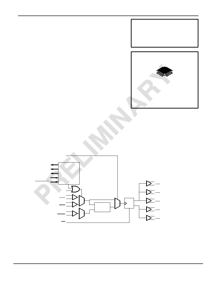
Figure 1. Block Diagram
CLK0
CLK1
Ext_FB
Sel_Clk
Dynamic Switch
Logic
PLL
PLL_En
÷2
÷4
Qb0
Qb1
Qb2
Qa0
Qa1
MR
Man_Override
Clk_Selected
Inp1bad
Inp0bad
Alarm_Reset
OR
200 -- 360 MHz
This document contains information on a product under development. Motorola reserves the right to change or discontinue this product without notice.
E
Motorola Inc. 2003
MPC99J93
FA SUFFIX
32--LEAD LQFP PACKAGE
CASE 873A
相关PDF资料 |
PDF描述 |
|---|---|
| MPDU281-2.0 | SILICON DELAY LINE, PDIP16 |
| MPDU282-2.0 | SILICON DELAY LINE, PDIP16 |
| MPDU482-4.5 | SILICON DELAY LINE, PDIP24 |
| MPDU882-4.5 | SILICON DELAY LINE, PDIP40 |
| MPDU482S-0.25 | SILICON DELAY LINE, DSO24 |
相关代理商/技术参数 |
参数描述 |
|---|---|
| MPCA06 | 制造商:Motorola Inc 功能描述: |
| MPCB-20.0-0-E563 | 制造商:TE Connectivity 功能描述:MPCB-20.0-0-E563 |
| MPCB-20.0-2 | 制造商:TE Connectivity 功能描述:MPCB-20.0-2 |
| MPCBL0001N04Q | 制造商:Intel 功能描述:KENNICOTT (NO FC, 2 X 2.0 GHZ) NO MEMORY OR HARD DRIVE, ROHS - Bulk |
| MPCBL0010N01Q | 制造商:Intel 功能描述:WAINWRIGHTBOARD - Bulk |
发布紧急采购,3分钟左右您将得到回复。