- 您现在的位置:买卖IC网 > PDF目录26839 > MPC99J93FAR2 (FREESCALE SEMICONDUCTOR INC) PLL BASED CLOCK DRIVER, 5 TRUE OUTPUT(S), 0 INVERTED OUTPUT(S), PQFP32 PDF资料下载
参数资料
| 型号: | MPC99J93FAR2 |
| 厂商: | FREESCALE SEMICONDUCTOR INC |
| 元件分类: | 时钟及定时 |
| 英文描述: | PLL BASED CLOCK DRIVER, 5 TRUE OUTPUT(S), 0 INVERTED OUTPUT(S), PQFP32 |
| 封装: | PLASTIC, LQFP-32 |
| 文件页数: | 2/8页 |
| 文件大小: | 213K |
| 代理商: | MPC99J93FAR2 |
MPC99J93
MOTOROLA TIMING SOLUTIONS
2
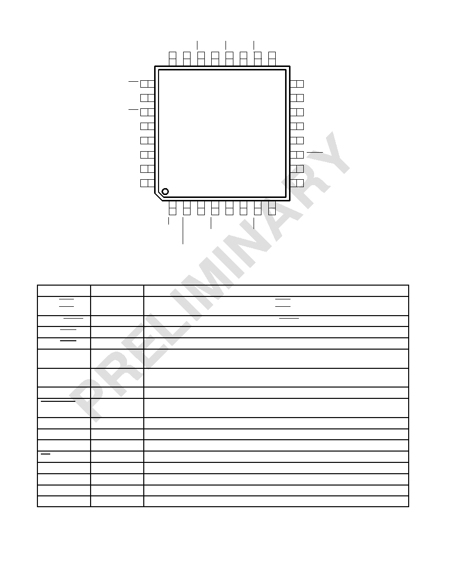
Figure 2. 32--Lead Pinout (Top View)
GND
VCC
Qb0
Qb1
Qb2
VCC
MR
Alar
m_Reset
CLK0
Sel_Clk
CLK1
GND
25
26
27
28
29
30
31
32
15
14
13
12
11
10
9
12345678
24
23
22
21
20
19
18
17
16
MPC99J93
Ext_FB
GND
Clk_Selected
Inp1bad
Inp0bad
VCC
PLL_En
Man_Override
VCC_PLL
VCC
Qa0
Qa1
Table 1. Pin Descriptions
Pin Name
I/O
Pin Definition
CLK0, CLK0
CLK1, CLK1
LVPECL Input
Differential PLL clock reference (CLK0 pulldown, CLK0 pullup)
Differential PLL clock reference (CLK1 pulldown, CLK1 pullup)
Ext_FB, Ext_FB
LVPECL Input
Differential PLL feedback clock (Ext_FB pulldown, Ext_FB pullup)
Qa0:1, Qa0:1
LVPECL Output
Differential 1x output pairs. Connect one QAx pair to Ext_FB.
Qb0:2, Qb0:2
LVPECL Output
Differential 2x output pairs
Inp0bad
LVCMOS Output
Indicates detection of a bad input reference clock 0 with respect to the feedback signal. The output
is active HIGH and will remain HIGH until the alarm reset is asserted
Inp1bad
LVCMOS Output
Indicates detection of a bad input reference clock 1 with respect to the feedback signal. The output
is active HIGH and will remain HIGH until the alarm reset is asserted
Clk_Selected
LVCMOS Output
‘0’ if clock 0 is selected, ‘1’ if clock 1 is selected
Alarm_Reset
LVCMOS Input
‘0’ will reset the input bad flags and align Clk_Selected with Sel_Clk. The input is “one--shotted”
(50k pullup)
Sel_Clk
LVCMOS Input
‘0’ selects CLK0, ‘1’ selects CLK1 (50k pulldown)
Manual_Override
LVCMOS Input
‘1’ disables internal clock switch circuitry (50k pulldown)
PLL_En
LVCMOS Input
‘0’ bypasses selected input reference around the phase--locked loop (50k pullup)
MR
LVCMOS Input
‘0’ resets the internal dividers forcing Q outputs LOW. Asynchronous to the clock (50k pullup)
VCCA
Power Supply
PLL power supply
VCC
Power Supply
Digital power supply
GNDA
Power Supply
PLL ground
GND
Power Supply
Digital ground
相关PDF资料 |
PDF描述 |
|---|---|
| MPDU281-2.0 | SILICON DELAY LINE, PDIP16 |
| MPDU282-2.0 | SILICON DELAY LINE, PDIP16 |
| MPDU482-4.5 | SILICON DELAY LINE, PDIP24 |
| MPDU882-4.5 | SILICON DELAY LINE, PDIP40 |
| MPDU482S-0.25 | SILICON DELAY LINE, DSO24 |
相关代理商/技术参数 |
参数描述 |
|---|---|
| MPCA06 | 制造商:Motorola Inc 功能描述: |
| MPCB-20.0-0-E563 | 制造商:TE Connectivity 功能描述:MPCB-20.0-0-E563 |
| MPCB-20.0-2 | 制造商:TE Connectivity 功能描述:MPCB-20.0-2 |
| MPCBL0001N04Q | 制造商:Intel 功能描述:KENNICOTT (NO FC, 2 X 2.0 GHZ) NO MEMORY OR HARD DRIVE, ROHS - Bulk |
| MPCBL0010N01Q | 制造商:Intel 功能描述:WAINWRIGHTBOARD - Bulk |
发布紧急采购,3分钟左右您将得到回复。