- 您现在的位置:买卖IC网 > PDF目录98031 > MPS6717RLRE (ON SEMICONDUCTOR) 500 mA, 80 V, NPN, Si, SMALL SIGNAL TRANSISTOR, TO-92 PDF资料下载
参数资料
| 型号: | MPS6717RLRE |
| 厂商: | ON SEMICONDUCTOR |
| 元件分类: | 小信号晶体管 |
| 英文描述: | 500 mA, 80 V, NPN, Si, SMALL SIGNAL TRANSISTOR, TO-92 |
| 封装: | PLASTIC, TO-226AE, 3 PIN |
| 文件页数: | 18/34页 |
| 文件大小: | 331K |
| 代理商: | MPS6717RLRE |
第1页第2页第3页第4页第5页第6页第7页第8页第9页第10页第11页第12页第13页第14页第15页第16页第17页当前第18页第19页第20页第21页第22页第23页第24页第25页第26页第27页第28页第29页第30页第31页第32页第33页第34页
9–13
Reliability and Quality Assurance
Motorola Small–Signal Transistors, FETs and Diodes Device Data
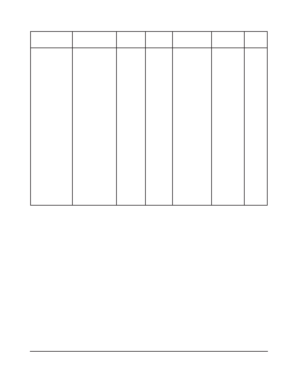
Table 1–2 – Time Dependent Failure Mechanisms in Semiconductor Devices
(Applicable to Discrete and Integrated Circuits)
Device
Association
Process
Relevant
Factors
Accelerating
Factors
Typical
Activation
Energy in eV
Model
Reference
Silicon Oxide
Silicon–Silicon
Oxide Interface
Metallization
Bond and Other
Mechanical Interfaces
Various Water Fab,
Assembly, and
Silicon Defects
Surface Charges
Inversion, Accumulation
Oxide Pinholes
Dielectric Breakdown
(TDDB)
Charge Loss
Electromigration
Corrosion
Chemical
Galvanic
Electrolytic
Intermetallic
Growth
Metal Scratches
Mask Defects, etc.
Silicon Defects
Mobile Ions
E/V, T
E, T
T, J
Grain Size
Doping
Contamination
T, Impurities
Bond Strength
T, V
E, T
J, T
H, E/V, T
T
T, V
1.0
0.7–1.0 (Bipolar)
1.0 (Bipolar)
0.3–0.4 (MOS)
0.3 (MOS)
0.8 (MOS)
EPROM
1.0 Large grain Al
(glassivated)
0.5
Small grain Al
0.7 Cu–Al/Cu–Si–Al
(sputtered)
0.6–0.7
(for electrolysis)
E/V may have
thresholds
1.0 (Au/Al)
0.5–0.7 eV
0.5 eV
Fitch, et al.
Peck
1984 WRS
Hokari, et al.
Domangue, et al.
Crook, D.L.
Gear, G.
Nanda, et al.
Black, J.R.
Lycoudes, N.E.
Fitch, W.T
Howes, et al.
MMPD
1A
2
18
5
3
4
11
6
7
12
8
9
10
13
V = voltage; E = electric field; T = temperature; J = current density; H = humidity
NO. REFERENCE
1A
1.0 eV activation for leakage type failures.
Fitch, W.T.; Greer, P.; Lycoudes, N.; ‘‘Data to Support 0.001%/1000
Hours for Plastic I/C’s.’’ Case study on linear product shows 0.914 eV
activation energy which is within experimental error of 0.9 to 1.3 eV
activation energies for reversible leakage (inversion) failures reported
in the literature.
1B
0.7 To 1.0 eV for oxide defect failures for bipolar structures. This is
under investigation subsequent to information obtained from 1984
Wafer Reliability Symposium, especially for bipolar capacitors with
silicon nitride as dielectric.
2
1.0 eV activation for leakage type failures.
Peck, D.S.; ‘‘New Concerns About Integrated Circuit Reliability’’ 1978
Reliability Physics Symposium.
3
0.36 eV for dielectric breakdown for MOS gate structures.
Domangue, E.; Rivera, R.; Shedard, C.; ‘‘Reliability Prediction Using
Large MOS Capacitors’’, 1984 Reliability Physics Symposium.
4
0.3 eV for dielectric breakdown.
Crook, D.L.; ‘‘Method of Determining Reliability Screens for Time
Dependent Dielectric Breakdown’’, 1979 Reliability Physics
Symposium.
5
1.0 eV for dielectric breakdown.
Hokari, Y.; et al.; IEDM Technical Digest, 1982.
6
1.0 eV for large grain Al–Si (compared to line width).
Nanda, Vangard, Gj–P; Black, J.R.; ‘‘Electromigration of Al–Si Alloy
Films’’, 1978 Reliability Physics Symposium.
7
0.5 eV Al, 0.7 eV Cu–Al small grain (compared to line width).
Black, J.R.; ‘‘Current Limitation of Thin Film Conductor’’ 1982 Reli-
ability Physics Symposium.
8
0.65 eV for corrosion mechanism.
Lycoudes, N.E.; ‘‘The Reliability of Plastic Microcircuits in Moist
Environments’’, 1978 Solid State Technology.
9
1.0 eV for open wires or high resistance bonds at the pad bond
due to Au–Al intermetallics.
Fitch, W.T.; ‘‘Operating Life vs Junction Temperatures for Plastic
Encapsulated I/C (1.5 mil Au wire)’’, unpublished report.
10
0.7 eV for assembly related defects.
Howes, M.G.; Morgan, D.V.; ‘‘Reliability and Degradation, Semi-
conductor Devices and CIrcuits’’ John Wiley and Sons, 1981.
11
Gear, G.; ‘‘FAMOUS PROM Reliability Studies’’, 1976 Reliability
Physics Symposium.
12
Black, J.R.: unpublished report.
13
Motorola Memory Products Division; unpublished report.
相关PDF资料 |
PDF描述 |
|---|---|
| MPS6717ZL1 | 500 mA, 80 V, NPN, Si, SMALL SIGNAL TRANSISTOR, TO-92 |
| MPS6724RLRE | 1000 mA, 40 V, NPN, Si, SMALL SIGNAL TRANSISTOR, TO-92 |
| MPS6725RL | 1000 mA, 50 V, NPN, Si, SMALL SIGNAL TRANSISTOR, TO-92 |
| MPS6725RLRA | 1000 mA, 50 V, NPN, Si, SMALL SIGNAL TRANSISTOR, TO-92 |
| MPS6725RL1 | 1000 mA, 50 V, NPN, Si, SMALL SIGNAL TRANSISTOR, TO-92 |
相关代理商/技术参数 |
参数描述 |
|---|---|
| MPS6724 | 功能描述:达林顿晶体管 1A 40V NPN RoHS:否 制造商:Texas Instruments 配置:Octal 晶体管极性:NPN 集电极—发射极最大电压 VCEO:50 V 发射极 - 基极电压 VEBO: 集电极—基极电压 VCBO: 最大直流电集电极电流:0.5 A 最大集电极截止电流: 功率耗散: 最大工作温度:+ 150 C 安装风格:SMD/SMT 封装 / 箱体:SOIC-18 封装:Reel |
| MPS6724G | 功能描述:达林顿晶体管 1A 40V NPN RoHS:否 制造商:Texas Instruments 配置:Octal 晶体管极性:NPN 集电极—发射极最大电压 VCEO:50 V 发射极 - 基极电压 VEBO: 集电极—基极电压 VCBO: 最大直流电集电极电流:0.5 A 最大集电极截止电流: 功率耗散: 最大工作温度:+ 150 C 安装风格:SMD/SMT 封装 / 箱体:SOIC-18 封装:Reel |
| MPS6724RLRA | 功能描述:达林顿晶体管 1A 40V NPN RoHS:否 制造商:Texas Instruments 配置:Octal 晶体管极性:NPN 集电极—发射极最大电压 VCEO:50 V 发射极 - 基极电压 VEBO: 集电极—基极电压 VCBO: 最大直流电集电极电流:0.5 A 最大集电极截止电流: 功率耗散: 最大工作温度:+ 150 C 安装风格:SMD/SMT 封装 / 箱体:SOIC-18 封装:Reel |
| MPS6724RLRAG | 功能描述:达林顿晶体管 1A 40V NPN RoHS:否 制造商:Texas Instruments 配置:Octal 晶体管极性:NPN 集电极—发射极最大电压 VCEO:50 V 发射极 - 基极电压 VEBO: 集电极—基极电压 VCBO: 最大直流电集电极电流:0.5 A 最大集电极截止电流: 功率耗散: 最大工作温度:+ 150 C 安装风格:SMD/SMT 封装 / 箱体:SOIC-18 封装:Reel |
| MPS6725 | 功能描述:达林顿晶体管 1A 50V NPN RoHS:否 制造商:Texas Instruments 配置:Octal 晶体管极性:NPN 集电极—发射极最大电压 VCEO:50 V 发射极 - 基极电压 VEBO: 集电极—基极电压 VCBO: 最大直流电集电极电流:0.5 A 最大集电极截止电流: 功率耗散: 最大工作温度:+ 150 C 安装风格:SMD/SMT 封装 / 箱体:SOIC-18 封装:Reel |
发布紧急采购,3分钟左右您将得到回复。