- 您现在的位置:买卖IC网 > PDF目录98034 > MPSA70RLRA (ON SEMICONDUCTOR) 100 mA, 40 V, PNP, Si, SMALL SIGNAL TRANSISTOR, TO-92 PDF资料下载
参数资料
| 型号: | MPSA70RLRA |
| 厂商: | ON SEMICONDUCTOR |
| 元件分类: | 小信号晶体管 |
| 英文描述: | 100 mA, 40 V, PNP, Si, SMALL SIGNAL TRANSISTOR, TO-92 |
| 封装: | PLASTIC, TO-226AA, 3 PIN |
| 文件页数: | 7/37页 |
| 文件大小: | 490K |
| 代理商: | MPSA70RLRA |
第1页第2页第3页第4页第5页第6页当前第7页第8页第9页第10页第11页第12页第13页第14页第15页第16页第17页第18页第19页第20页第21页第22页第23页第24页第25页第26页第27页第28页第29页第30页第31页第32页第33页第34页第35页第36页第37页
Surface Mount Information
7–10
Motorola Small–Signal Transistors, FETs and Diodes Device Data
INFORMATION FOR USING SURFACE MOUNT PACKAGES
RECOMMENDED FOOTPRINTS FOR SURFACE MOUNTED APPLICATIONS
Surface mount board layout is a critical portion of the total
design. The footprint for the semiconductor packages must
be the correct size to ensure proper solder connection inter-
face between the board and the package. With the correct
pad geometry, the packages will self align when subjected to
a solder reflow process.
POWER DISSIPATION FOR A SURFACE MOUNT DEVICE
The power dissipation for a surface mount device is a func-
tion of the drain/collector pad size. These can vary from the
minimum pad size for soldering to a pad size given for
maximum power dissipation. Power dissipation for a surface
mount device is determined by TJ(max), the maximum rated
junction temperature of the die, R
θJA, the thermal resistance
from the device junction to ambient, and the operating
temperature, TA. Using the values provided on the data
sheet, PD can be calculated as follows:
PD =
TJ(max) – TA
R
θJA
The values for the equation are found in the maximum
ratings table on the data sheet. Substituting these values into
the equation for an ambient temperature TA of 25°C, one can
calculate the power dissipation of the device. For example,
for a SOT–223 device, PD is calculated as follows.
PD =
150
°C – 25°C
156
°C/W
= 800 milliwatts
The 156
°C/W for the SOT–223 package assumes the use
of the recommended footprint on a glass epoxy printed circuit
board to achieve a power dissipation of 800 milliwatts. There
are other alternatives to achieving higher power dissipation
from the surface mount packages. One is to increase the
area of the drain/collector pad. By increasing the area of the
drain/collector pad, the power dissipation can be increased.
Although the power dissipation can almost be doubled with
this method, area is taken up on the printed circuit board
which can defeat the purpose of using surface mount
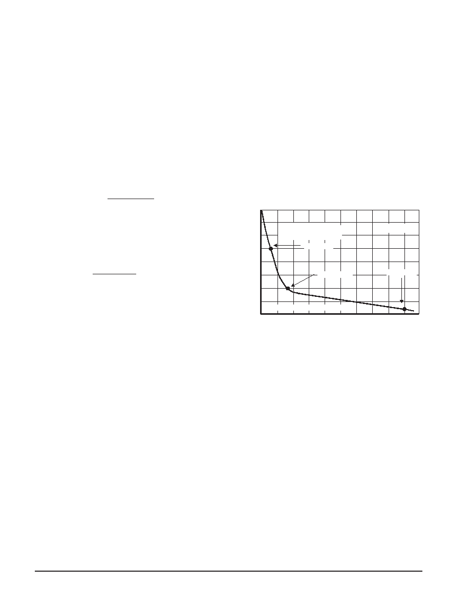
technology. For example, a graph of R
θJA versus drain pad
area is shown in Figure 1.
Another alternative would be to use a ceramic substrate or
an aluminum core board such as Thermal Clad
. Using a
board material such as Thermal Clad, an aluminum core
board, the power dissipation can be doubled using the same
footprint.
T
O
AMBIENT
(
C/W)°
R
JA
,THERMAL
RE
S
IS
TANCE
,J
U
NCTI
O
N
θ
0.8 Watts
1.25 Watts*
1.5 Watts
A, AREA (SQUARE INCHES)
0.0
0.2
0.4
0.6
0.8
1.0
160
140
120
100
80
Board Material = 0.0625
″
G–10/FR–4, 2 oz Copper
TA = 25°C
*Mounted on the DPAK footprint
Figure 1. Thermal Resistance versus Drain Pad
Area for the SOT–223 Package (Typical)
SOLDER STENCIL GUIDELINES
Prior to placing surface mount components onto a printed
circuit board, solder paste must be applied to the pads.
Solder stencils are used to screen the optimum amount.
These stencils are typically 0.008 inches thick and may be
made of brass or stainless steel. For packages such as the
SOT–23, SC–59, SC–70/SOT–323, SC–90/SOT–416,
SOD–123, SOT–223, SOT–363, SO–14, SO–16, and
TSOP–6 packages, the stencil opening should be the same
as the pad size or a 1:1 registration.
相关PDF资料 |
PDF描述 |
|---|---|
| MPSA70RL | 100 mA, 40 V, PNP, Si, SMALL SIGNAL TRANSISTOR, TO-92 |
| MPSA70RL1 | 100 mA, 40 V, PNP, Si, SMALL SIGNAL TRANSISTOR, TO-92 |
| MPSA92J18Z | 500 mA, 300 V, PNP, Si, SMALL SIGNAL TRANSISTOR |
| MPSA92L34Z | 500 mA, 300 V, PNP, Si, SMALL SIGNAL TRANSISTOR, TO-92 |
| MPSA92D75Z | 500 mA, 300 V, PNP, Si, SMALL SIGNAL TRANSISTOR, TO-92 |
相关代理商/技术参数 |
参数描述 |
|---|---|
| MPSA70RLRM | 功能描述:两极晶体管 - BJT 100mA 40V PNP RoHS:否 制造商:STMicroelectronics 配置: 晶体管极性:PNP 集电极—基极电压 VCBO: 集电极—发射极最大电压 VCEO:- 40 V 发射极 - 基极电压 VEBO:- 6 V 集电极—射极饱和电压: 最大直流电集电极电流: 增益带宽产品fT: 直流集电极/Base Gain hfe Min:100 A 最大工作温度: 安装风格:SMD/SMT 封装 / 箱体:PowerFLAT 2 x 2 |
| MPSA70RLRMG | 功能描述:两极晶体管 - BJT 100mA 40V PNP RoHS:否 制造商:STMicroelectronics 配置: 晶体管极性:PNP 集电极—基极电压 VCBO: 集电极—发射极最大电压 VCEO:- 40 V 发射极 - 基极电压 VEBO:- 6 V 集电极—射极饱和电压: 最大直流电集电极电流: 增益带宽产品fT: 直流集电极/Base Gain hfe Min:100 A 最大工作温度: 安装风格:SMD/SMT 封装 / 箱体:PowerFLAT 2 x 2 |
| MPSA75 | 制造商:CENTRAL 制造商全称:Central Semiconductor Corp 功能描述:Small Signal Transistors |
| MPSA75_06 | 制造商:ONSEMI 制造商全称:ON Semiconductor 功能描述:Darlington Transistors PNP Silicon |
| MPSA75RLRA | 功能描述:达林顿晶体管 500mA 40V PNP RoHS:否 制造商:Texas Instruments 配置:Octal 晶体管极性:NPN 集电极—发射极最大电压 VCEO:50 V 发射极 - 基极电压 VEBO: 集电极—基极电压 VCBO: 最大直流电集电极电流:0.5 A 最大集电极截止电流: 功率耗散: 最大工作温度:+ 150 C 安装风格:SMD/SMT 封装 / 箱体:SOIC-18 封装:Reel |
发布紧急采购,3分钟左右您将得到回复。