- 您现在的位置:买卖IC网 > PDF目录21704 > MRF6S21100MR1 (Freescale Semiconductor)MOSFET RF N-CH 28V 23W TO270-4 PDF资料下载
参数资料
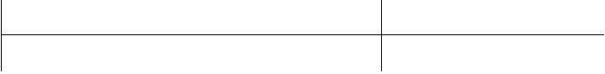
| 型号: | MRF6S21100MR1 |
| 厂商: | Freescale Semiconductor |
| 文件页数: | 12/20页 |
| 文件大小: | 1456K |
| 描述: | MOSFET RF N-CH 28V 23W TO270-4 |
| 标准包装: | 500 |
| 晶体管类型: | LDMOS |
| 频率: | 2.11GHz |
| 增益: | 14.5dB |
| 电压 - 测试: | 28V |
| 额定电流: | 10µA |
| 电流 - 测试: | 1.05A |
| 功率 - 输出: | 23W |
| 电压 - 额定: | 68V |
| 封装/外壳: | TO-270-4 |
| 供应商设备封装: | TO-270 WB-4 |
| 包装: | 带卷 (TR) |
2�
� RF Device Data�
� Freescale Semiconductor�
� MRF6S21100NR1 MRF6S21100NBR1�
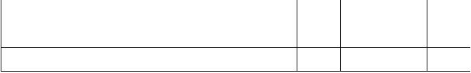
� Table 3. ESD Protection Characteristics�
� Test Methodology�
� Class�
� Human Body Model (per JESD22--A114)�
� 1B (Minimum)�
� Machine Model (per EIA/JESD22--A115)�
� A (Minimum)�
� Charge Device Model (per JESD22--C101)�
� IV (Minimum)�
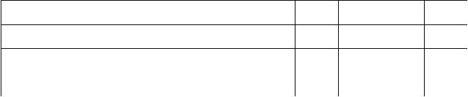
� Table 4. Moisture Sensitivity Level�
� Test Methodology�
� Rating�
� Package Peak Temperature�
� Unit�
� Per JESD22--A113, IPC/JEDEC J--STD--020�
� 3�
� 260�
� °C�
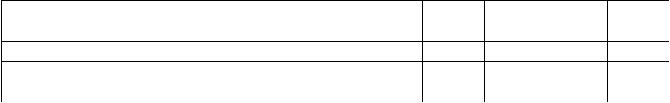
� Table 5. Electrical Characteristics�
� (TA�
� =25°C unless otherwise noted)�
� Characteristic�
� Symbol�
� Min�
� Typ�
� Max�
� Unit�
� Off Characteristics�
� Zero Gate Voltage Drain Leakage Current�
� (VDS�
� =68Vdc,VGS�
� =0Vdc)�
� IDSS�
� ?�
� ?�
� 10�
� μAdc�
� Zero Gate Voltage Drain Leakage Current�
� (VDS�
� =28Vdc,VGS�
� =0Vdc)�
� IDSS�
� ?�
� ?�
� 1�
� μAdc�
� Gate--Source Leakage Current�
� (VGS�
� =5Vdc,VDS�
� =0Vdc)�
� IGSS�
� ?�
� ?�
� 1�
� μAdc�
� On Characteristics�
� Gate Threshold Voltage�
� (VDS�
� =10Vdc,ID�
� = 330�
� μAdc)�
� VGS(th)�
� 1�
� 2�
� 3�
� Vdc�
� Gate Quiescent Voltage�
� (VDS�
� =28Vdc,ID�
� = 1050 mAdc)�
� VGS(Q)�
� ?�
� 2.8�
� ?�
� Vdc�
� Fixture Gate Quiescent Voltage�
� (1)�
� (VDD�
� =28Vdc,ID�
� = 1050 mAdc, Measured in Functional Test)�
� VGG(Q)�
� 2.2�
� 3.1�
� 4.4�
� Vdc�
� Drain--Source On--Voltage�
� (VGS�
� =10Vdc,ID�
� =3.3Adc)�
� VDS(on)�
� ?�
� 0.24�
� ?�
� Vdc�
� Dynamic Characteristics�
� (2)�
� Reverse Transfer Capacitance�
� (VDS�
� =28Vdc±�
� 30 mV(rms)ac @ 1 MHz, VGS�
� =0Vdc)�
� Crss�
� ?�
� 1.5�
� ?�
� pF�
� Functional Tests�
� (In Freescale Test Fixture, 50 ohm system) VDD�
� =28Vdc,IDQ�
� = 1050 mA, Pout�
� =23WAvg.,f1=2112.5MHz,f2=�
� 2157.5 MHz, 2--carrier W--CDMA, 3.84 MHz Channel Bandwidth Carriers, ACPR measured in 3.84 MHz Channel Bandwidth @�
� ±5MHz�
� Offset. IM3 measured in 3.84 MHz Bandwidth @�
� ±10 MHz Offset. PAR = 8.5 dB @ 0.01% Probability on CCDF.�
� Power Gain�
� Gps�
� 13�
� 14.5�
� 16�
� dB�
� Drain Efficiency�
� ηD�
� 24�
� 25.5�
� 36�
� %�
� Intermodulation Distortion�
� IM3�
� -- 4 7�
� -- 3 7�
� -- 3 5�
� dBc�
� Adjacent Channel Power Ratio�
� ACPR�
� -- 5 0�
� -- 4 0�
� -- 3 8�
� dBc�
� Input Return Loss�
� IRL�
� ?�
� -- 1 2�
� -- 1 0�
� dB�
� 1. VGG�
� = 11/10 x VGS(Q). Parameter measured on Freescale Test Fixture, due to resistive divider network on the board. Refer to Test Circuit�
� schematic.�
� 2. Part is internally matched both on input and output.�
� LIFETIME BU�
� Y�
� LAST ORDER 1 JUL 11 LAST SHIP 30 JUN 12�
�  �
�
� � �  �
�
� � �  �
�
� � �  �
�
� �  �
�
� � �  �
�
� � �  �
�
� � �  �
�
� � �  �
�
� � �  �
�
� � 相关PDF资料 |
PDF描述 |
|---|---|
| C3391-66.000 | OSC 66.000 MHZ 3.3V +/-25PPM SMD |
| MRF6S21100MBR1 | MOSFET RF N-CH 28V 23W TO272-4 |
| C3391-64.000 | OSC 64.000 MHZ 3.3V +/-25PPM SMD |
| 150333K1000FE | CAP FILM 0.033UF 1KVDC AXIAL |
| C3391-60.000 | OSC 60.000 MHZ 3.3V +/-25PPM SMD |
相关代理商/技术参数 |
参数描述 |
|---|---|
| MRF6S21100NBR1 | 功能描述:射频MOSFET电源晶体管 2170MHZ 23W RoHS:否 制造商:Freescale Semiconductor 配置:Single 晶体管极性: 频率:1800 MHz to 2000 MHz 增益:27 dB 输出功率:100 W 汲极/源极击穿电压: 漏极连续电流: 闸/源击穿电压: 最大工作温度: 封装 / 箱体:NI-780-4 封装:Tray |
| MRF6S21100NR1 | 功能描述:射频MOSFET电源晶体管 2170MHZ 23W RoHS:否 制造商:Freescale Semiconductor 配置:Single 晶体管极性: 频率:1800 MHz to 2000 MHz 增益:27 dB 输出功率:100 W 汲极/源极击穿电压: 漏极连续电流: 闸/源击穿电压: 最大工作温度: 封装 / 箱体:NI-780-4 封装:Tray |
| MRF6S21100NR1_08 | 制造商:FREESCALE 制造商全称:Freescale Semiconductor, Inc 功能描述:RF Power Field Effect Transistors N-Channel Enhancement-Mode Lateral MOSFETs |
| MRF6S21140HR3 | 功能描述:射频MOSFET电源晶体管 HV6 LDMOS 30W NI880H RoHS:否 制造商:Freescale Semiconductor 配置:Single 晶体管极性: 频率:1800 MHz to 2000 MHz 增益:27 dB 输出功率:100 W 汲极/源极击穿电压: 漏极连续电流: 闸/源击穿电压: 最大工作温度: 封装 / 箱体:NI-780-4 封装:Tray |
| MRF6S21140HR3_07 | 制造商:FREESCALE 制造商全称:Freescale Semiconductor, Inc 功能描述:RF Power Field Effect Transistors N-Channel Enhancement-Mode Lateral MOSFETs |
发布紧急采购,3分钟左右您将得到回复。