- 您现在的位置:买卖IC网 > PDF目录80578 > MSC8122TMP4800V (FREESCALE SEMICONDUCTOR INC) 32-BIT, 300 MHz, OTHER DSP, PBGA431 PDF资料下载
参数资料
| 型号: | MSC8122TMP4800V |
| 厂商: | FREESCALE SEMICONDUCTOR INC |
| 元件分类: | 数字信号处理 |
| 英文描述: | 32-BIT, 300 MHz, OTHER DSP, PBGA431 |
| 封装: | FCBGA-431 |
| 文件页数: | 35/48页 |
| 文件大小: | 1158K |
| 代理商: | MSC8122TMP4800V |
第1页第2页第3页第4页第5页第6页第7页第8页第9页第10页第11页第12页第13页第14页第15页第16页第17页第18页第19页第20页第21页第22页第23页第24页第25页第26页第27页第28页第29页第30页第31页第32页第33页第34页当前第35页第36页第37页第38页第39页第40页第41页第42页第43页第44页第45页第46页第47页第48页
MSC8122 Quad Digital Signal Processor Data Sheet, Rev. 16
Hardware Design Considerations
Freescale Semiconductor
40
Never allow VDD to exceed VDDH + 0.8V.
Design the VDDH supply to prevent reverse current flow by adding a minimum 10 Ω resistor to GND to limit the
current. Such a design yields an initial VDDH level of VDD – 0.8 V before it is enabled.
After power-up, VDDH must not exceed VDD/VCCSYN by more than 2.6 V.
3.2
When used as a drop-in replacement in MSC8102 applications or when implementing a new design, use the guidelines
described in Migrating Designs from the MSC8102 to the MSC8122 (AN2716) and the MSC8122 Design Checklist (AN3374
for optimal system performance. MSC8122 and MSC8126 Power Circuit Design Recommendations and Examples (AN2937)
provides detailed design information. See Section 2.5.2 for start-up timing specifications.
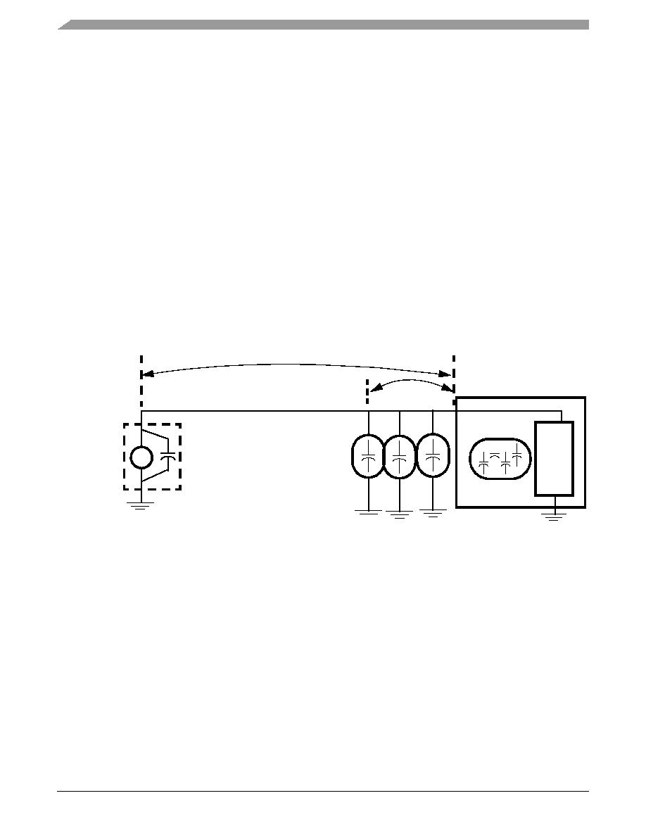
Figure 33 shows the recommended power decoupling circuit for the core power supply. The voltage regulator and the
decoupling capacitors should supply the required device current without any drop in voltage on the device pins. The voltage on
the package pins should not drop below the minimum specified voltage level even for a very short spikes. This can be achieved
by using the following guidelines:
For the core supply, use a voltage regulator rated at 1.2 V with nominal rating of at least 3 A. This rating does not
reflect actual average current draw, but is recommended because it resists changes imposed by transient spikes and has
better voltage recovery time than supplies with lower current ratings.
Decouple the supply using low-ESR capacitors mounted as close as possible to the socket. Figure 33 shows three
capacitors in parallel to reduce the resistance. Three capacitors is a recommended minimum number. If possible, mount
at least one of the capacitors directly below the MSC8122 device.
Each VCC and VDD pin on the MSC8122 device should have a low-impedance path to the board power supply. Similarly, each
GND
pin should have a low-impedance path to the ground plane. The power supply pins drive distinct groups of logic on the
chip. The VCC power supply should have at least four 0.1 F by-pass capacitors to ground located as closely as possible to the
four sides of the package. The capacitor leads and associated printed circuit traces connecting to chip VCC, VDD, and GND should
be kept to less than half an inch per capacitor lead. A four-layer board is recommended, employing two inner layers as VCC and
GND
planes.
All output pins on the MSC8122 have fast rise and fall times. PCB trace interconnection length should be minimized to
minimize undershoot and reflections caused by these fast output switching times. This recommendation particularly applies to
the address and data buses. Maximum PCB trace lengths of six inches are recommended. For the DSI control signals in
synchronous mode, ensure that the layout supports the DSI AC timing requirements and minimizes any signal crosstalk.
Capacitance calculations should consider all device loads as well as parasitic capacitances due to the PCB traces. Attention to
proper PCB layout and bypassing becomes especially critical in systems with higher capacitive loads because these loads create
higher transient currents in the VCC, VDD, and GND circuits. Pull up all unused inputs or signals that will be inputs during reset.
Special care should be taken to minimize the noise levels on the PLL supply pins. There is one pair of PLL supply pins:
VCCSYN-GNDSYN. To ensure internal clock stability, filter the power to the VCCSYN input with a circuit similar to the one in
Figure 33. Core Power Supply Decoupling
+
-
Power supply
or
Voltage Regulator
High frequency capacitors
(very low ESR and ESL)
Bulk/Tantalum capacitors
with low ESR and ESL
MSC8122
Maximum IR drop
of 15 mV at 1 A
Note: Use at least three capacitors.
Lmax = 2 cm
One 0.01 F capacitor
for every 3 core supply
(Imin = 3 A)
pads.
1.2 V
Each capacitor must be at least 150
μF.
相关PDF资料 |
PDF描述 |
|---|---|
| MPC8545CVUATGA | 32-BIT, 1200 MHz, MICROPROCESSOR, CBGA783 |
| MPC8545VTAQG | 32-BIT, 1000 MHz, MICROPROCESSOR, PBGA783 |
| MPC8547CHXATJ | 32-BIT, 1200 MHz, MICROPROCESSOR, CBGA783 |
| MPC8547CVTAUGA | 32-BIT, 1000 MHz, MICROPROCESSOR, PBGA783 |
| MPC8547ECHXAUGB | 32-BIT, 1000 MHz, MICROPROCESSOR, CBGA783 |
相关代理商/技术参数 |
参数描述 |
|---|---|
| MSC8122TMP6400 | 功能描述:数字信号处理器和控制器 - DSP, DSC PBGA PB 1.2V 105C 400MHZ RoHS:否 制造商:Microchip Technology 核心:dsPIC 数据总线宽度:16 bit 程序存储器大小:16 KB 数据 RAM 大小:2 KB 最大时钟频率:40 MHz 可编程输入/输出端数量:35 定时器数量:3 设备每秒兆指令数:50 MIPs 工作电源电压:3.3 V 最大工作温度:+ 85 C 封装 / 箱体:TQFP-44 安装风格:SMD/SMT |
| MSC8122TMP6400V | 功能描述:DSP 16BIT 400MHZ MULTI 431FCPBGA RoHS:否 类别:集成电路 (IC) >> 嵌入式 - DSP(数字式信号处理器) 系列:StarCore 标准包装:2 系列:StarCore 类型:SC140 内核 接口:DSI,以太网,RS-232 时钟速率:400MHz 非易失内存:外部 芯片上RAM:1.436MB 电压 - 输入/输出:3.30V 电压 - 核心:1.20V 工作温度:-40°C ~ 105°C 安装类型:表面贴装 封装/外壳:431-BFBGA,FCBGA 供应商设备封装:431-FCPBGA(20x20) 包装:托盘 |
| MSC8122TVT4800V | 功能描述:IC DSP QUAD 16B 300MHZ 431FCPBGA RoHS:是 类别:集成电路 (IC) >> 嵌入式 - DSP(数字式信号处理器) 系列:StarCore 标准包装:2 系列:StarCore 类型:SC140 内核 接口:DSI,以太网,RS-232 时钟速率:400MHz 非易失内存:外部 芯片上RAM:1.436MB 电压 - 输入/输出:3.30V 电压 - 核心:1.20V 工作温度:-40°C ~ 105°C 安装类型:表面贴装 封装/外壳:431-BFBGA,FCBGA 供应商设备封装:431-FCPBGA(20x20) 包装:托盘 |
| MSC8122TVT6400 | 功能描述:DSP 16BIT 400MHZ MULTI 431FCPBGA RoHS:是 类别:集成电路 (IC) >> 嵌入式 - DSP(数字式信号处理器) 系列:StarCore 标准包装:2 系列:StarCore 类型:SC140 内核 接口:DSI,以太网,RS-232 时钟速率:400MHz 非易失内存:外部 芯片上RAM:1.436MB 电压 - 输入/输出:3.30V 电压 - 核心:1.20V 工作温度:-40°C ~ 105°C 安装类型:表面贴装 封装/外壳:431-BFBGA,FCBGA 供应商设备封装:431-FCPBGA(20x20) 包装:托盘 |
| MSC8122TVT6400V | 功能描述:IC DSP QUAD 16B 400MHZ 431FCPBGA RoHS:是 类别:集成电路 (IC) >> 嵌入式 - DSP(数字式信号处理器) 系列:StarCore 标准包装:2 系列:StarCore 类型:SC140 内核 接口:DSI,以太网,RS-232 时钟速率:400MHz 非易失内存:外部 芯片上RAM:1.436MB 电压 - 输入/输出:3.30V 电压 - 核心:1.20V 工作温度:-40°C ~ 105°C 安装类型:表面贴装 封装/外壳:431-BFBGA,FCBGA 供应商设备封装:431-FCPBGA(20x20) 包装:托盘 |
发布紧急采购,3分钟左右您将得到回复。