- 您现在的位置:买卖IC网 > PDF目录378677 > MSD601RT1 (Motorola, Inc.) NPN General Purpose Amplifier Transistors Surface Mount PDF资料下载
参数资料
| 型号: | MSD601RT1 |
| 厂商: | Motorola, Inc. |
| 英文描述: | NPN General Purpose Amplifier Transistors Surface Mount |
| 中文描述: | npn型通用放大器,晶体管表面贴装 |
| 文件页数: | 2/4页 |
| 文件大小: | 110K |
| 代理商: | MSD601RT1 |
2
Motorola Small–Signal Transistors, FETs and Diodes Device Data
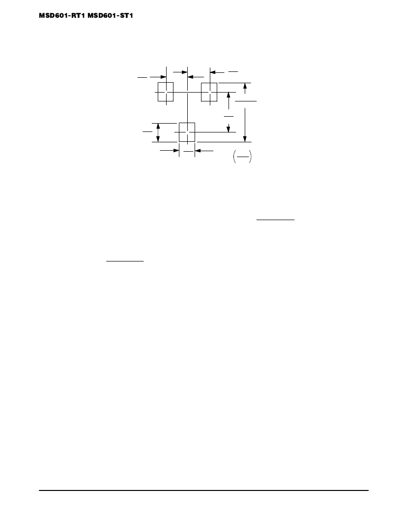
MINIMUM RECOMMENDED FOOTPRINT FOR SURFACE MOUNTED APPLICATIONS
Surface mount board layout is a critical portion of the total
design. The footprint for the semiconductor packages must
be the correct size to insure proper solder connection
interface between the board and the package. With the
correct pad geometry, the packages will self align when
subjected to a solder reflow process.
mm
inches
2.5–3.0
0.039
1.0
0.094
2.4
0.8
0.098–0.118
0.031
0.95
0.037
0.95
0.037
SC–59 POWER DISSIPATION
The power dissipation of the SC–59 is a function of the pad
size. This can vary from the minimum pad size for soldering
to the pad size given for maximum power dissipation. Power
dissipation for a surface mount device is determined by
TJ(max), the maximum rated junction temperature of the die,
R
θ
JA, the thermal resistance from the device junction to
ambient; and the operating temperature, TA. Using the
values provided on the data sheet, PD can be calculated as
follows:
PD =
TJ(max) – TA
R
θ
JA
The values for the equation are found in the maximum
ratings table on the data sheet. Substituting these values into
the equation for an ambient temperature TA of 25
°
C, one can
calculate the power dissipation of the device which in this
case is 200 milliwatts.
PD =150
°
C – 25
°
C
625
°
C/W
= 200 milliwatts
The 625
°
C/W assumes the use of the recommended
footprint on a glass epoxy printed circuit board to achieve a
power dissipation of 200 milliwatts. Another alternative would
be to use a ceramic substrate or an aluminum core board
such as Thermal Clad
. Using a board material such as
Thermal Clad, a power dissipation of 400 milliwatts can be
achieved using the same footprint.
SOLDERING PRECAUTIONS
The melting temperature of solder is higher than the rated
temperature of the device. When the entire device is heated
to a high temperature, failure to complete soldering within a
short time could result in device failure. Therefore, the
following items should always be observed in order to
minimize the thermal stress to which the devices are
subjected.
Always preheat the device.
The delta temperature between the preheat and
soldering should be 100
°
C or less.*
When preheating and soldering, the temperature of the
leads and the case must not exceed the maximum
temperature ratings as shown on the data sheet. When
using infrared heating with the reflow soldering method,
the difference should be a maximum of 10
°
C.
The soldering temperature and time should not exceed
260
°
C for more than 10 seconds.
When shifting from preheating to soldering, the
maximum temperature gradient should be 5
°
C or less.
After soldering has been completed, the device should
be allowed to cool naturally for at least three minutes.
Gradual cooling should be used as the use of forced
cooling will increase the temperature gradient and result
in latent failure due to mechanical stress.
Mechanical stress or shock should not be applied during
cooling
* Soldering a device without preheating can cause excessive
thermal shock and stress which can result in damage to the
device.
相关PDF资料 |
PDF描述 |
|---|---|
| MSM5116160B | 1M×16 Dynamic RAM(1M×16动态RAM) |
| MSM5116160F | 1,048,576-Word 】 16-Bit DYNAMIC RAM : FAST PAGE MODE TYPE |
| MSM5116160F-50JS | 1,048,576-Word 】 16-Bit DYNAMIC RAM : FAST PAGE MODE TYPE |
| MSM5116160F-50TS-K | 1,048,576-Word 】 16-Bit DYNAMIC RAM : FAST PAGE MODE TYPE |
| MSM5116160F-60JS | 1,048,576-Word 】 16-Bit DYNAMIC RAM : FAST PAGE MODE TYPE |
相关代理商/技术参数 |
参数描述 |
|---|---|
| MSD-601RT1 | 制造商:ONSEMI 制造商全称:ON Semiconductor 功能描述:NPN General Purpose Amplifier Transistors Surface Mount |
| MSD601-RT1 | 功能描述:两极晶体管 - BJT 100mA 60V NPN RoHS:否 制造商:STMicroelectronics 配置: 晶体管极性:PNP 集电极—基极电压 VCBO: 集电极—发射极最大电压 VCEO:- 40 V 发射极 - 基极电压 VEBO:- 6 V 集电极—射极饱和电压: 最大直流电集电极电流: 增益带宽产品fT: 直流集电极/Base Gain hfe Min:100 A 最大工作温度: 安装风格:SMD/SMT 封装 / 箱体:PowerFLAT 2 x 2 |
| MSD-601RT1G | 制造商:ONSEMI 制造商全称:ON Semiconductor 功能描述:NPN General Purpose Amplifier Transistors Surface Mount |
| MSD601-RT1G | 功能描述:两极晶体管 - BJT 100mA 60V NPN RoHS:否 制造商:STMicroelectronics 配置: 晶体管极性:PNP 集电极—基极电压 VCBO: 集电极—发射极最大电压 VCEO:- 40 V 发射极 - 基极电压 VEBO:- 6 V 集电极—射极饱和电压: 最大直流电集电极电流: 增益带宽产品fT: 直流集电极/Base Gain hfe Min:100 A 最大工作温度: 安装风格:SMD/SMT 封装 / 箱体:PowerFLAT 2 x 2 |
| MSD601-RT2 | 制造商:Rochester Electronics LLC 功能描述:- Bulk 制造商:ON Semiconductor 功能描述: |
发布紧急采购,3分钟左右您将得到回复。