- 您现在的位置:买卖IC网 > PDF目录299520 > MSK5143ZS (MS KENNEDY CORP) 1.21 V-20 V ADJUSTABLE POSITIVE LDO REGULATOR, 0.55 V DROPOUT, CSFM5 PDF资料下载
参数资料
| 型号: | MSK5143ZS |
| 厂商: | MS KENNEDY CORP |
| 元件分类: | 可调正电压单路输出LDO稳压器 |
| 英文描述: | 1.21 V-20 V ADJUSTABLE POSITIVE LDO REGULATOR, 0.55 V DROPOUT, CSFM5 |
| 封装: | HERMETIC SEALED, SIP-5 |
| 文件页数: | 3/8页 |
| 文件大小: | 463K |
| 代理商: | MSK5143ZS |
APPLICATION NOTES
3
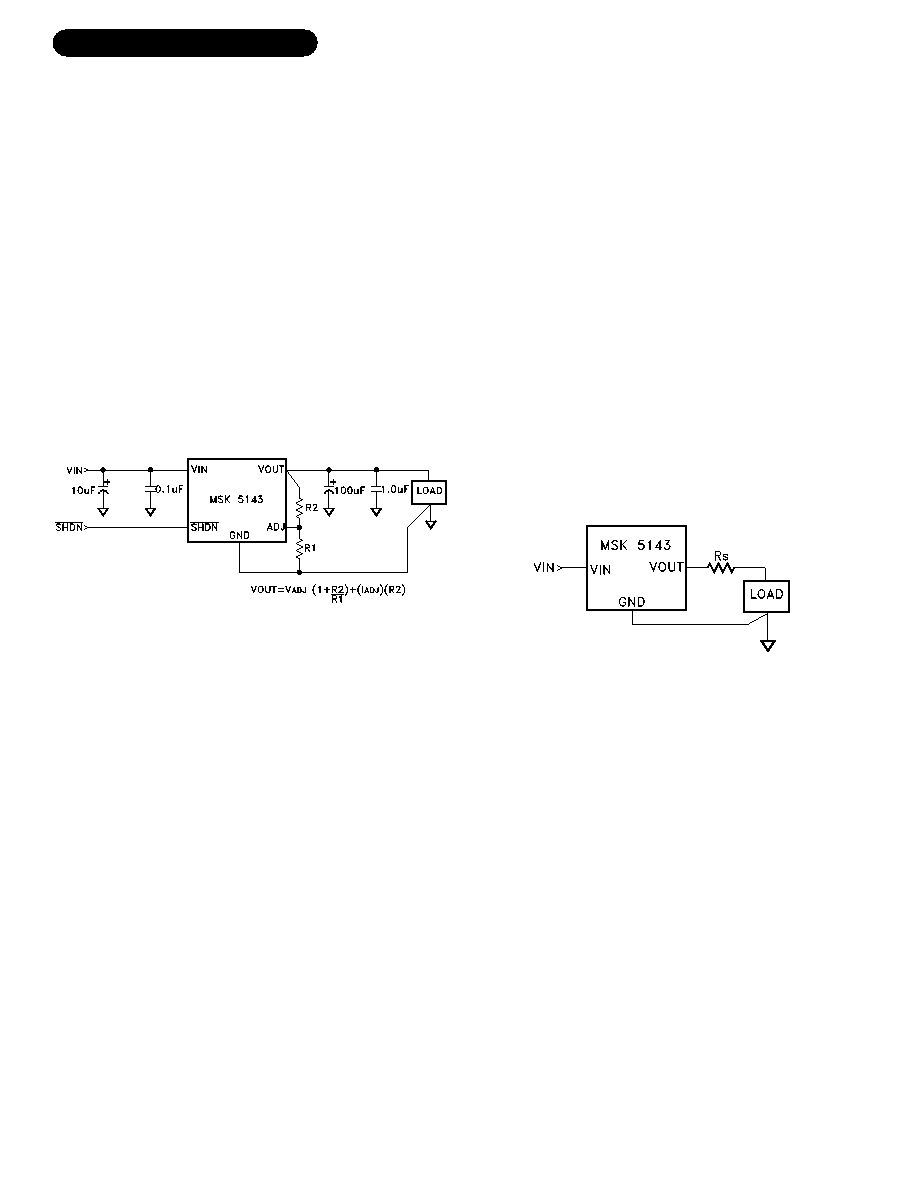
INPUT BYPASS CAPACITORS
Unless the regulator is located very close to the main input
filter capacitor, a 1μF to 10μF low ESR tantalum capacitor
should be added to the regulator's input to maximize tran-
sient response and minimize power supply transients. A
0.1μF ceramic capacitor should also be used for high fre-
quency bypassing.
FIGURE 1
OUTPUT CAPACITOR SELECTION
For most applications a 10μF low ESR tantalum capacitor,
as close to the regulators output as possible, is all that is
required for the MSK 5143 to be stable. When using a 10μF
capacitor on the lower output voltage devices, a minimum
ESR is required of the capacitor. This requirement decreases
from 20mΩ for VOUT ≤ 1.5V to 5mΩ for VOUT ≥ 3.3V.
With an increase in capacitance, the minimum ESR require-
ment decreases. At 100μF, the minimum ESR requirement
decreases to 5mΩ for all versions of the MSK 5143. To
reduce ringing and improve transient response, capacitors
with slightly larger ESR in the range of 20mΩ to 50mΩ pro-
vides improved damping. Capacitors with higher ESR can
be combined in parallel with low ESR ceramic capacitors for
good high frequency response and settling time. The maxi-
mum ESR value must be less than 3Ω. Care must be taken
when selecting a ceramic type. The X5R and X7R are the
best choice for output stability when considering response
due to applied voltage and temperature.
LOAD REGULATION
In voltage regulator applications where very large load cur-
rents are present, the load connection is very important. The
path connecting the output of the regulator to the load must
be extremely low impedance to avoid affecting the load regu-
lation specifications. As shown in figure 2, any impedance
(Rs) in this path will form a voltage divider with the load. For
best results the ground pin should be connected directly to
the load as shown in figure 2. The direct connection elimi-
nates the effect the potential voltage drop in the power ground
path can have on the internal ground sensing, thus improving
load regulation. The MSK 5143 ground pin trace must be
designed to carry the ground pin current without significant
voltage drops. See typical performance curves.
FIGURE 2
OVERLOAD PROTECTION
The MSK 5143 regulator features both current limit and ther-
mal overload protection. Within the safe operating region,
the regulator will current limit above the 3A amp rating. As
the input to output voltage increases, however, the current
limit decreases to keep the output transistor within its power
dissipation limitation. See the Current Limit Typical Curves
for conditional performance detail. If the device heats enough
to exceed its rated die junction temperature due to exces-
sive ambient temperature, improper heat sinking etc., the
regulator will shutdown until an appropriate junction tempera-
ture is maintained. To bring the regulator out of shutdown,
the device input may need to be cycled to zero and power
reapplied to eliminate the shutdown condition.
REVERSE VOLTAGE PROTECTION
The regulators are protected against reverse input and out-
put voltages. Reverse input voltages up to 20V will be blocked
from the input while current flow is limited to less than 1mA.
The reverse voltage on the input is also prevented from ap-
pearing on the output and the load. When the input voltage is
pulled down to ground and the output is held up by a second
source, the current flow between them is limited to typically
600μA. See the electrical specifications table.
OUTPUT ADJUST
The output voltage range of the MSK 5143 is 1.21V to 20V.
The output voltage is set by the ratio of two external resis-
tors as shown in Figure 1. The device monitors the output to
maintain the voltage at the ADJ pin. The ADJ pin is the input
to the error amplifier. It has a bias current of 3μA which
flows through R2 into the pin. The ADJ pin voltage is 1.21V
referenced to ground. The value of R1 should be less than
4.17K to minimize errors in the output voltage caused by
the ADJ pin bias current. Reference the typical performance
curves for load regulation variation due to the change in the
output voltage.
SHUTDOWN MODE
The SHDN pin is used to put the regulator into its low power
state. The output will be off when the SHDN pin is pulled
low. Quiescent current drops from 1mA to less the 1μA in
shutdown mode. The SHDN pin can be driven by 5V logic or
open-collector logic with a pull-up resistor. The typical SHDN
pin current is 3uA. Connect the SHDN pin to VIN if not used.
If the SHDN pin is not connected, the regulator will go into a
low power shutdown state.
Rev. B 8/11
相关PDF资料 |
PDF描述 |
|---|---|
| MSK5144-1.5H | ADJUSTABLE POSITIVE LDO REGULATOR, BCC3 |
| MSK5144-1.8H | ADJUSTABLE POSITIVE LDO REGULATOR, BCC3 |
| MSKD200-16 | 200 A, 1600 V, SILICON, RECTIFIER DIODE |
| MSAD200-16 | 200 A, 1600 V, SILICON, RECTIFIER DIODE |
| MSM4256K-35 | 256K X 4 STANDARD SRAM, 35 ns, CDIP28 |
相关代理商/技术参数 |
参数描述 |
|---|---|
| MSK5150-00ETD | 制造商:MSK 制造商全称:M.S. Kennedy Corporation 功能描述:VERY HIGH CURRENT, LOW DROPOUT VOLTAGE REGULATORS |
| MSK5150-00ETS | 制造商:MSK 制造商全称:M.S. Kennedy Corporation 功能描述:VERY HIGH CURRENT, LOW DROPOUT VOLTAGE REGULATORS |
| MSK5150-00ETU | 制造商:MSK 制造商全称:M.S. Kennedy Corporation 功能描述:VERY HIGH CURRENT, LOW DROPOUT VOLTAGE REGULATORS |
| MSK5150-00EZD | 制造商:MSK 制造商全称:M.S. Kennedy Corporation 功能描述:VERY HIGH CURRENT, LOW DROPOUT VOLTAGE REGULATORS |
| MSK5150-00EZS | 制造商:MSK 制造商全称:M.S. Kennedy Corporation 功能描述:VERY HIGH CURRENT, LOW DROPOUT VOLTAGE REGULATORS |
发布紧急采购,3分钟左右您将得到回复。