- 您现在的位置:买卖IC网 > PDF目录299520 > MSK5143ZS (MS KENNEDY CORP) 1.21 V-20 V ADJUSTABLE POSITIVE LDO REGULATOR, 0.55 V DROPOUT, CSFM5 PDF资料下载
参数资料
| 型号: | MSK5143ZS |
| 厂商: | MS KENNEDY CORP |
| 元件分类: | 可调正电压单路输出LDO稳压器 |
| 英文描述: | 1.21 V-20 V ADJUSTABLE POSITIVE LDO REGULATOR, 0.55 V DROPOUT, CSFM5 |
| 封装: | HERMETIC SEALED, SIP-5 |
| 文件页数: | 4/8页 |
| 文件大小: | 463K |
| 代理商: | MSK5143ZS |
To select a heat sink for the MSK 5143, the following for-
mula for convective heat flow may be used.
Governing Equation:
TJ = PD X (RθJC + RθCS + RθSA) + TA
Where
TJ
= Junction Temperature
PD
= Total Power Dissipation
RθJC = Junction to Case Thermal Resistance
RθCS = Case to Heat Sink Thermal Resistance
RθSA = Heat Sink to Ambient Thermal Resistance
TA
= Ambient Temperature
Power Dissipation=(VIN-VOUT) x IOUT
Next, the user must select a maximum junction tempera-
ture. The absolute maximum allowable junction temperature
is 150°C. The equation may now be rearranged to solve for
the required heat sink to ambient thermal resistance (RθSA).
Example:
An MSK 5143 is connected for VIN=+5V and
VOUT=+3.3V. IOUT is a continuous 2.5A DC level. The
ambient temperature is +25°C. The maximum desired junc-
tion temperature is +125°C.
RθJC=2.3°C/W and RθCS=0.15°C/W for most thermal
greases
Power Dissipation=(5V-3.3V) x (2.5A)
=4.25 Watts
Solve for RθSA:
125°C - 25°C
4.25W
= 21.1°C/W
In this example, a heat sink with a thermal resistance of no
more than 21.1°C/W must be used to maintain a maximum
junction temperature of no more than 125°C.
VIN min=Minimum input voltage
VOUT max=Maximum output voltage across the full
VDROP=Worst case dropout voltage (Typically 340mV)
IOUT peak=Maximum load current
GND Pin Current=Max. GND Pin Current at IOUT peak
APPLICATION NOTES CONT'D
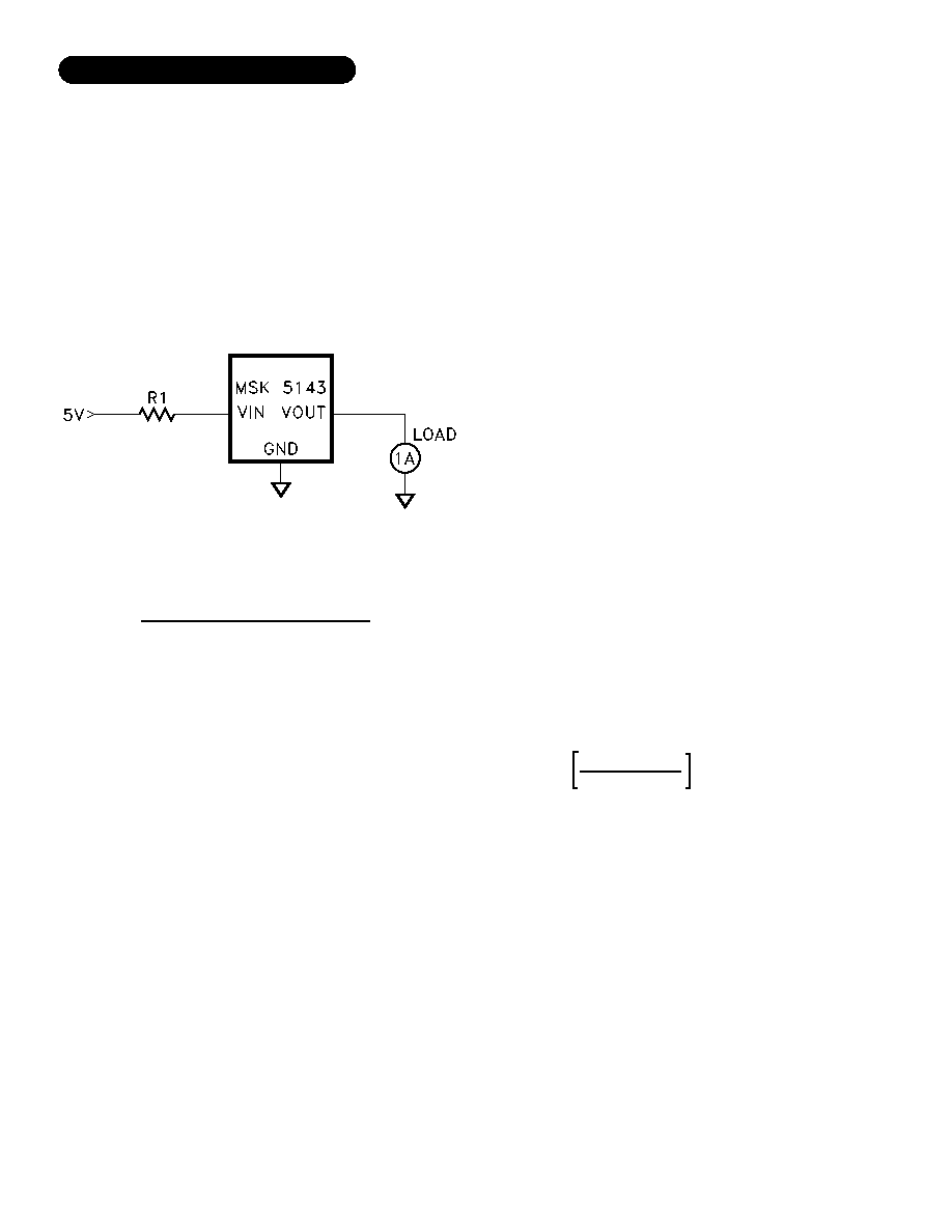
MINIMIZING POWER DISSIPATION:
To maximize the performance and reduce power dissipation
of the MSK 5143 device, VIN should be maintained as close
to dropout or at VIN minimum when possible. See Input Sup-
ply Voltage requirements. A series resistor can be used to
lower VIN close to the dropout specification, lowering the
input to output voltage differential. In turn, this will decrease
the power that the device is required to dissipate. Knowing
peak current requirements and worst case voltages, a re-
sistor can be selected that will drop a portion of the excess
voltage and help to distribute the heating. The circuit below
illustrates this method.
The maximum resistor value can be calculated from the
following:
R1 max =
Where:
VIN min - (VOUT max + VDROP)
IOUT peak + GND Pin Current
Temperature range
RθSA=
- 2.3°C/W - 0.15°C/W
HEAT SINK SELECTION
4
Rev. B 8/11
相关PDF资料 |
PDF描述 |
|---|---|
| MSK5144-1.5H | ADJUSTABLE POSITIVE LDO REGULATOR, BCC3 |
| MSK5144-1.8H | ADJUSTABLE POSITIVE LDO REGULATOR, BCC3 |
| MSKD200-16 | 200 A, 1600 V, SILICON, RECTIFIER DIODE |
| MSAD200-16 | 200 A, 1600 V, SILICON, RECTIFIER DIODE |
| MSM4256K-35 | 256K X 4 STANDARD SRAM, 35 ns, CDIP28 |
相关代理商/技术参数 |
参数描述 |
|---|---|
| MSK5150-00ETD | 制造商:MSK 制造商全称:M.S. Kennedy Corporation 功能描述:VERY HIGH CURRENT, LOW DROPOUT VOLTAGE REGULATORS |
| MSK5150-00ETS | 制造商:MSK 制造商全称:M.S. Kennedy Corporation 功能描述:VERY HIGH CURRENT, LOW DROPOUT VOLTAGE REGULATORS |
| MSK5150-00ETU | 制造商:MSK 制造商全称:M.S. Kennedy Corporation 功能描述:VERY HIGH CURRENT, LOW DROPOUT VOLTAGE REGULATORS |
| MSK5150-00EZD | 制造商:MSK 制造商全称:M.S. Kennedy Corporation 功能描述:VERY HIGH CURRENT, LOW DROPOUT VOLTAGE REGULATORS |
| MSK5150-00EZS | 制造商:MSK 制造商全称:M.S. Kennedy Corporation 功能描述:VERY HIGH CURRENT, LOW DROPOUT VOLTAGE REGULATORS |
发布紧急采购,3分钟左右您将得到回复。