- 您现在的位置:买卖IC网 > PDF目录80482 > MSP430G2433IRHB32T (TEXAS INSTRUMENTS INC) 16-BIT, FLASH, 16 MHz, RISC MICROCONTROLLER, PQCC32 PDF资料下载
参数资料
| 型号: | MSP430G2433IRHB32T |
| 厂商: | TEXAS INSTRUMENTS INC |
| 元件分类: | 微控制器/微处理器 |
| 英文描述: | 16-BIT, FLASH, 16 MHz, RISC MICROCONTROLLER, PQCC32 |
| 封装: | GREEN, PLASTIC, QFN-32 |
| 文件页数: | 9/63页 |
| 文件大小: | 831K |
| 代理商: | MSP430G2433IRHB32T |
第1页第2页第3页第4页第5页第6页第7页第8页当前第9页第10页第11页第12页第13页第14页第15页第16页第17页第18页第19页第20页第21页第22页第23页第24页第25页第26页第27页第28页第29页第30页第31页第32页第33页第34页第35页第36页第37页第38页第39页第40页第41页第42页第43页第44页第45页第46页第47页第48页第49页第50页第51页第52页第53页第54页第55页第56页第57页第58页第59页第60页第61页第62页第63页
Supply voltage range,
during flash memory
programming
Supply voltage range,
during program execution
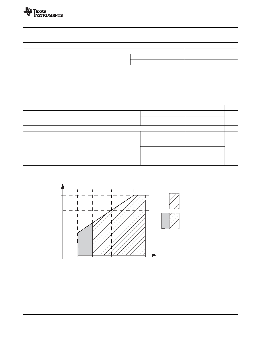
Legend :
16 MHz
System
Frequency
-
MHz
12 MHz
6 MHz
1.8 V
Supply Voltage - V
3.3 V
2.7 V
2.2 V
3.6 V
MSP430G2x33
MSP430G2x03
SLAS734C
– APRIL 2011 – REVISED AUGUST 2011
Absolute Maximum Ratings
(1)
Voltage applied at VCC to VSS
–0.3 V to 4.1 V
Voltage applied to any pin(2)
–0.3 V to VCC + 0.3 V
Diode current at any device pin
±2 mA
Unprogrammed device
–55°C to 150°C
Storage temperature range, Tstg
(3)
Programmed device
–55°C to 150°C
(1)
Stresses beyond those listed under
"absolute maximum ratings" may cause permanent damage to the device. These are stress ratings
only, and functional operation of the device at these or any other conditions beyond those indicated under
"recommended operating
conditions
" is not implied. Exposure to absolute-maximum-rated conditions for extended periods may affect device reliability.
(2)
All voltages referenced to VSS. The JTAG fuse-blow voltage, VFB, is allowed to exceed the absolute maximum rating. The voltage is
applied to the TEST pin when blowing the JTAG fuse.
(3)
Higher temperature may be applied during board soldering according to the current JEDEC J-STD-020 specification with peak reflow
temperatures not higher than classified on the device label on the shipping boxes or reels.
Recommended Operating Conditions
MIN
NOM
MAX
UNIT
During program execution
1.8
3.6
VCC
Supply voltage
V
During flash
2.2
3.6
programming/erase
VSS
Supply voltage
0
V
TA
Operating free-air temperature
I version
–40
85
°C
VCC = 1.8 V,
dc
6
Duty cycle = 50%
± 10%
Processor frequency (maximum MCLK frequency using the
VCC = 2.7 V,
fSYSTEM
dc
12
MHz
USART module)(1)(2)
Duty cycle = 50%
± 10%
VCC = 3.3 V,
dc
16
Duty cycle = 50%
± 10%
(1)
The MSP430 CPU is clocked directly with MCLK. Both the high and low phase of MCLK must not exceed the pulse width of the
specified maximum frequency.
(2)
Modules might have a different maximum input clock specification. See the specification of the respective module in this data sheet.
Note:
Minimum processor frequency is defined by system clock. Flash program or erase operations require a minimum VCC
of 2.2 V.
Figure 1. Safe Operating Area
Copyright
2011, Texas Instruments Incorporated
17
相关PDF资料 |
PDF描述 |
|---|---|
| MK40DN512ZVMC10R | FLASH, 100 MHz, RISC MICROCONTROLLER, PBGA121 |
| MPC5604PEF0VLL6 | 32-BIT, FLASH, 64 MHz, MICROCONTROLLER, PQFP100 |
| MPC5604PFF0MLQ6 | 32-BIT, FLASH, 64 MHz, MICROCONTROLLER, PQFP144 |
| MPC5607BF0ACMG6R | 32-BIT, FLASH, 64 MHz, MICROCONTROLLER, PBGA208 |
| MPC8560PX833JD | 32-BIT, 833 MHz, RISC PROCESSOR, PBGA783 |
相关代理商/技术参数 |
参数描述 |
|---|---|
| MSP430G2444IDA38 | 制造商:Texas Instruments 功能描述:IC MCU 16BIT 8KB FLASH 38TSSOP 制造商:Texas Instruments 功能描述:CPU |
| MSP430G2444IDA38R | 制造商:Texas Instruments 功能描述:IC MCU 16BIT 8KB FLASH 38TSSOP 制造商:Texas Instruments 功能描述:CPU |
| MSP430G2444IRHA40R | 制造商:Texas Instruments 功能描述:IC MCU 16BIT 8KB FLASH 40VQFN |
| MSP430G2444IRHA40T | 制造商:Texas Instruments 功能描述:IC MCU 16BIT 8KB FLASH 40VQFN |
| MSP430G2444IYFFR | 制造商:Texas Instruments 功能描述:IC MCU 16BIT 8KB FLASH 49DSBGA 制造商:Texas Instruments 功能描述:Vaule Line |
发布紧急采购,3分钟左右您将得到回复。