- 您现在的位置:买卖IC网 > PDF目录229297 > MT5C2561EC-45IT (AUSTIN SEMICONDUCTOR INC) 256K X 1 STANDARD SRAM, 45 ns, CQCC28 PDF资料下载
参数资料
| 型号: | MT5C2561EC-45IT |
| 厂商: | AUSTIN SEMICONDUCTOR INC |
| 元件分类: | SRAM |
| 英文描述: | 256K X 1 STANDARD SRAM, 45 ns, CQCC28 |
| 封装: | CERAMIC, LCC-28 |
| 文件页数: | 7/11页 |
| 文件大小: | 81K |
| 代理商: | MT5C2561EC-45IT |
SRAM
MT5C2561
MT5C2561
Rev. 2.6 06/05
Austin Semiconductor, Inc. reserves the right to change products or specifications without notice.
5
Austin Semiconductor, Inc.
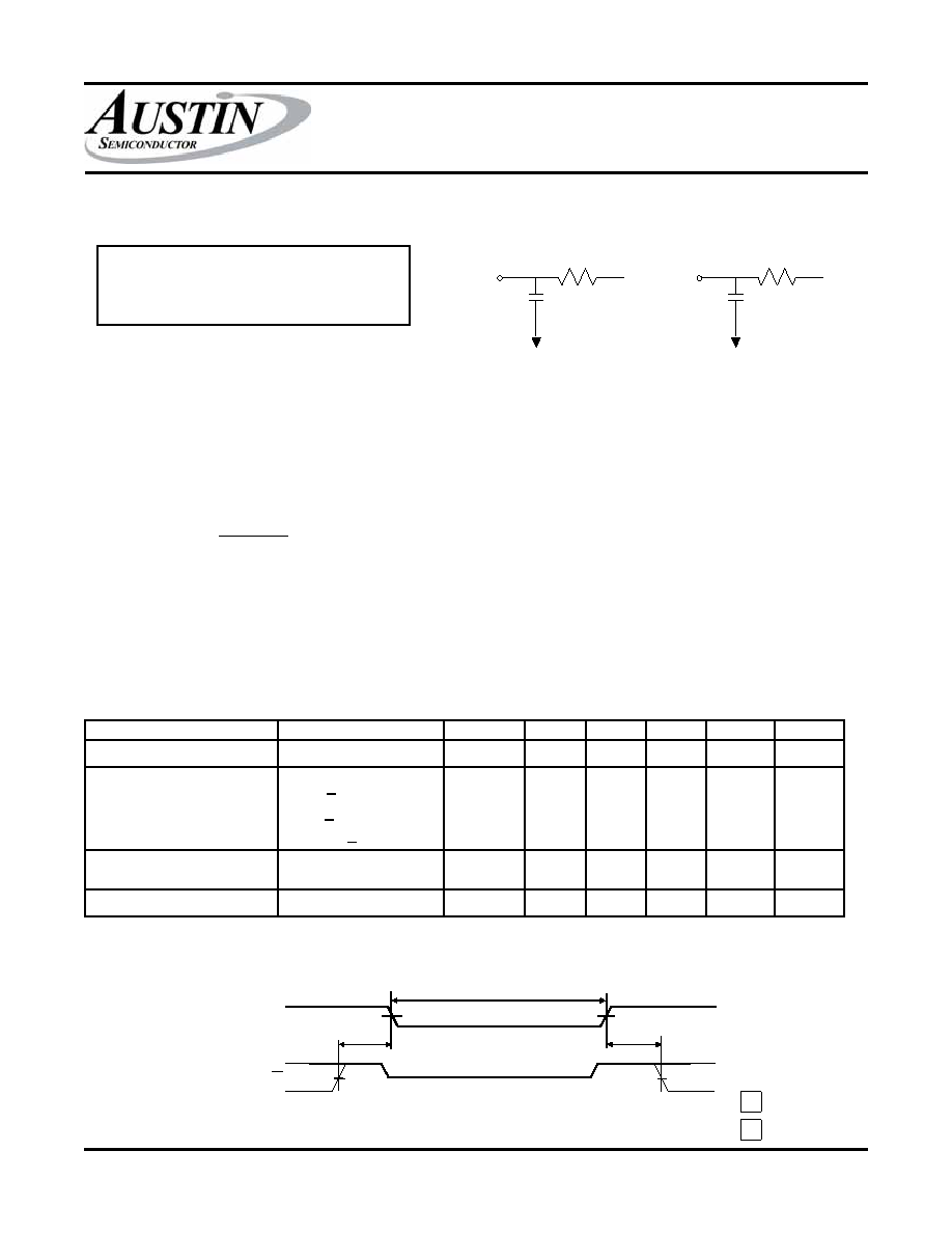
ACTEST CONDITIONS
Input pulse levels ...................................... Vss to 3.0V
Input rise and fall times ......................................... 5ns
Input timing reference levels ................................ 1.5V
Output reference levels ....................................... 1.5V
Output load ................................. See Figures 1 and 2
NOTES
1.
All voltages referenced to V
SS (GND).
2.
-3V for pulse width < 20ns
3.
I
CC is dependent on output loading and cycle rates.
The specified value applies with the outputs
unloaded, and f =
1
Hz.
tRC (MIN)
4.
This parameter is guaranteed but not tested.
5.
Test conditions as specified with the output loading
as shown in Fig. 1 unless otherwise noted.
6.
t
LZCE
, t
LZWE
, t
LZOE
, t
HZCE
, t
HZOE
and t
HZWE
are
specified with CL = 5pF as in Fig. 2. Transition is
measured ±200mV typical from steady state voltage,
allowing for actual tester RC time constant.
7.
At any given temperature and voltage condition, t
HZCE
is
less than t
LZCE
, and t
HZWE
is less than t
LZWE
and t
HZOE
is
less than t
LZOE
.
8.
WE\ is HIGH for READ cycle.
9.
Device is continuously selected. Chip enable is held in
its active state.
10. Address valid prior to, or coincident with, latest
occurring chip enable.
11. t
RC
= Read Cycle Time.
12. Chip enable (CE\) and write enable (WE\) can initiate and
terminate a WRITE cycle.
Fig. 1 Output Load
Equivalent
Fig. 2 Output Load
Equivalent
DATA RETENTION ELECTRICAL CHARACTERISTICS (L Version Only)
123
1234
DON’T CARE
UNDEFINED
LOW Vcc DATA RETENTION WAVEFORM
V
TH
= 1.73V
Q
167
30pF
V
TH
= 1.73V
Q
167
5pF
12345678
123
1234
123456789
123
1234
DATA RETENTION MODE
V
DR > 2V
4.5V
V
DR
t
CDR
t
R
V
IH
V
IL
V
CC
CE\
DESCRIPTION
CONDITIONS
SYM
MIN
MAX
UNITS
NOTES
VCC for Retention Data
VDR
2
---
V
Data Retention Current
CE\ > (VCC - 0.2V)
VIN > (VCC - 0.2V)
or < 0.2V
VCC = 2V
ICCDR
900
A
Chip Deselect to Data
Retention Time
tCDR
0
---
ns
4
Operation Recovery Time
tR
tRC
ns
4, 11
相关PDF资料 |
PDF描述 |
|---|---|
| M378T3253FG0-CE6 | 32M X 64 DDR DRAM MODULE, 0.45 ns, DMA240 |
| M93C06-DS3TG | 16 X 16 MICROWIRE BUS SERIAL EEPROM, PDSO8 |
| M93C06-WDS7 | 16 X 16 MICROWIRE BUS SERIAL EEPROM, PDSO8 |
| MT2VDDT832UY-75XX | 8M X 32 DDR DRAM MODULE, 0.75 ns, DMA100 |
| MB84VD22183EA-85PBS | SPECIALTY MEMORY CIRCUIT, PBGA71 |
相关代理商/技术参数 |
参数描述 |
|---|---|
| MT5C2564C-20/883C | 制造商:Micross Components, Inc. 功能描述:SRAM, 256KB - Rail/Tube |
| MT5C2564C-20/IT | 制造商:Micross Components 功能描述:SRAM, 256KB - Rail/Tube |
| MT5C2564C-20/XT | 制造商:Micross Components 功能描述:SRAM, 256KB - Rail/Tube |
| MT5C2564C-20L/883C | 制造商:Micross Components 功能描述:SRAM, 256KB - Rail/Tube |
| MT5C2564C-20L/IT | 制造商:Micross Components 功能描述:SRAM, 256KB - Rail/Tube |
发布紧急采购,3分钟左右您将得到回复。