- 您现在的位置:买卖IC网 > PDF目录96091 > MTB3N60E (ON SEMICONDUCTOR) 3 A, 600 V, 2.2 ohm, N-CHANNEL, Si, POWER, MOSFET PDF资料下载
参数资料
| 型号: | MTB3N60E |
| 厂商: | ON SEMICONDUCTOR |
| 元件分类: | JFETs |
| 英文描述: | 3 A, 600 V, 2.2 ohm, N-CHANNEL, Si, POWER, MOSFET |
| 文件页数: | 1/4页 |
| 文件大小: | 74K |
| 代理商: | MTB3N60E |
1
Motorola TMOS Power MOSFET Transistor Device Data
Product Preview
TMOS E-FET.
High Energy Power FET
D2PAK for Surface Mount
N–Channel Enhancement–Mode Silicon Gate
This advanced high voltage TMOS E–FET is designed to
withstand high energy in the avalanche mode and switch efficiently.
This new high energy device also offers a drain–to–source diode
with fast recovery time. Designed for high voltage, high speed
switching applications such as power supplies, PWM motor
controls and other inductive loads, the avalanche energy capability
is specified to eliminate the guesswork in designs where inductive
loads are switched and offer additional safety margin against
unexpected voltage transients.
Avalanche Energy Capability Specified at Elevated
Temperature
Low Stored Gate Charge for Efficient Switching
Internal Source–to–Drain Diode Designed to Replace External
Zener Transient Suppressor — Absorbs High Energy in the
Avalanche Mode
Source–to–Drain Diode Recovery Time Comparable to Discrete
Fast Recovery Diode
MAXIMUM RATINGS (TC = 25°C unless otherwise noted)
Rating
Symbol
Value
Unit
Drain–Source Voltage
VDSS
600
Vdc
Drain–Gate Voltage (RGS = 1.0 M)
VDGR
600
Vdc
Gate–Source Voltage — Continuous
Gate–Source Voltage — Non–repetitive
VGS
VGSM
±20
±40
Vdc
Vpk
Drain Current — Continuous
Drain Current — Continuous @ 100
°C
Drain Current — Pulsed
ID
IDM
3.0
2.4
14
Adc
Total Power Dissipation @ TC = 25°C
Derate above 25
°C
Total Power Dissipation @ TA = 25°C(1)
PD
75
0.6
2.5
Watts
W/
°C
Watts
Operating and Storage Temperature Range
TJ, Tstg
– 55 to 150
°C
UNCLAMPED DRAIN–TO–SOURCE AVALANCHE CHARACTERISTICS (TJ < 150°C)
Single Pulse Drain–to–Source Avalanche Energy — TJ = 25°C
Single Pulse Drain–to–Source Avalanche Energy — TJ = 100°C
Repetitive Pulse Drain–to–Source Avalanche Energy
WDSR(2)
WDSR(3)
290
46
7.5
mJ
THERMAL CHARACTERISTICS
Thermal Resistance — Junction to Case
°
Thermal Resistance — Junction to Ambient
°
Thermal Resistance — Junction to Ambient(1)
R
θJC
R
θJA
R
θJA
1.67
62.5
50
°C/W
Maximum Lead Temperature for Soldering Purposes, 1/8
″ from case for 10 seconds
TL
260
°C
(1) When surface mounted to an FR–4 board using the minimum recommended pad size
(2) VDD = 50 V, ID = 3.0 A
(3) Pulse Width and frequency is limited by TJ(max) and thermal response
This document contains information on a product under development. Motorola reserves the right to change or discontinue this product without notice.
E–FET and Designer’s are trademarks of Motorola, Inc. TMOS is a registered trademark of Motorola, Inc.
Preferred devices are Motorola recommended choices for future use and best overall value.
Order this document
by MTB3N60E/D
MOTOROLA
SEMICONDUCTOR TECHNICAL DATA
MTB3N60E
TMOS POWER FET
3.0 AMPERES
600 VOLTS
RDS(on) = 2.2 OHMS
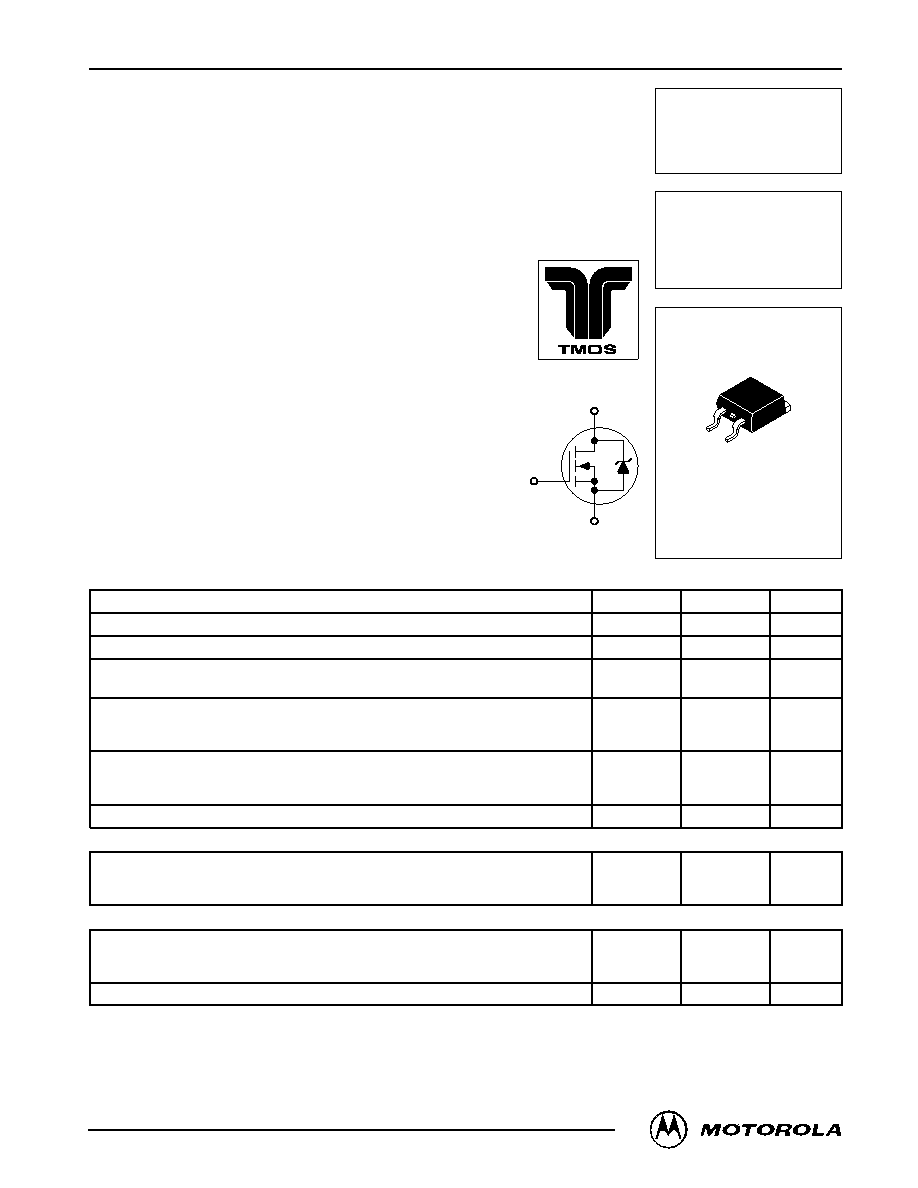
D
S
G
CASE 418B–03, Style 2
D2PAK
Motorola Preferred Device
Motorola, Inc. 1997
相关PDF资料 |
PDF描述 |
|---|---|
| MTB4N80ET4 | 4 A, 800 V, 3 ohm, N-CHANNEL, Si, POWER, MOSFET |
| MTB50N06V | 42 A, 60 V, 0.028 ohm, N-CHANNEL, Si, POWER, MOSFET |
| MTB50N06VT4 | 42 A, 60 V, 0.028 ohm, N-CHANNEL, Si, POWER, MOSFET |
| MTB55N06ZT4 | 55 A, 60 V, 0.016 ohm, N-CHANNEL, Si, POWER, MOSFET |
| MTB55N10EL | 55 A, 100 V, 0.03 ohm, N-CHANNEL, Si, POWER, MOSFET |
相关代理商/技术参数 |
参数描述 |
|---|---|
| MTB3N60ET4 | 制造商:Rochester Electronics LLC 功能描述:- Bulk 制造商:ON Semiconductor 功能描述: |
| MTB406N | 功能描述:拨动开关 4PDT TOGGLE SWITCH Decorat Bat Actuator RoHS:否 制造商:C&K Components 触点形式:DPDT 开关功能:ON - ON - ON 电流额定值: 电压额定值 AC:20 V 电压额定值 DC:20 V 功率额定值:0.4 VA 端接类型:V-Bracket 安装风格: 端子密封:Epoxy 触点电镀:Gold 照明:Not Illuminated |
| MTB40N10E | 制造商:ON Semiconductor 功能描述:Trans MOSFET N-CH 100V 40A 3-Pin(2+Tab) D2PAK Rail |
| MTB40N10ET4 | 制造商:ON Semiconductor 功能描述:Trans MOSFET N-CH 100V 40A 3-Pin(2+Tab) D2PAK T/R |
| MTB44P04J3 | 制造商:CYSTEKEC 制造商全称:Cystech Electonics Corp. 功能描述:P-Channel Enhancement Mode Power MOSFET |
发布紧急采购,3分钟左右您将得到回复。