- 您现在的位置:买卖IC网 > Datasheet目录480 > MTB75N05HDT4 (ON Semiconductor)MOSFET N-CH 50V 75A D2PAK-3 Datasheet资料下载
参数资料
| 型号: | MTB75N05HDT4 |
| 厂商: | ON Semiconductor |
| 文件页数: | 1/8页 |
| 文件大小: | 0K |
| 描述: | MOSFET N-CH 50V 75A D2PAK-3 |
| 产品变化通告: | Product Obsolescence 01/Apr/2004 |
| 标准包装: | 800 |
| FET 型: | MOSFET N 通道,金属氧化物 |
| FET 特点: | 标准 |
| 漏极至源极电压(Vdss): | 50V |
| 电流 - 连续漏极(Id) @ 25° C: | 75A |
| 开态Rds(最大)@ Id, Vgs @ 25° C: | 9.5 毫欧 @ 20A,10V |
| Id 时的 Vgs(th)(最大): | 4V @ 250µA |
| 闸电荷(Qg) @ Vgs: | 100nC @ 10V |
| 输入电容 (Ciss) @ Vds: | 3900pF @ 25V |
| 功率 - 最大: | 2.5W |
| 安装类型: | 表面贴装 |
| 封装/外壳: | TO-263-3,D²Pak(2 引线+接片),TO-263AB |
| 供应商设备封装: | D2PAK |
| 包装: | 带卷 (TR) |
| 其它名称: | MTB75N05HDT4OS |
�� �
�
�MTB75N05HD�
�Preferred� Device�
�Power� MOSFET�
�75� Amps,� 50� Volts�
�N� ?� Channel� D� 2� PAK�
�This� Power� MOSFET� is� designed� to� withstand� high� energy� in� the�
�avalanche� and� commutation� modes.� The� energy� efficient� design� also�
�offers� a� drain� ?� to� ?� source� diode� with� a� fast� recovery� time.� Designed� for�
�low� voltage,� high� speed� switching� applications� in� power� supplies,�
�converters� and� PWM� motor� controls,� these� devices� are� particularly�
�well� suited� for� bridge� circuits� where� diode� speed� and� commutating�
�safe� operating� areas� are� critical� and� offer� additional� safety� margin�
�against� unexpected� voltage� transients.�
�?� Avalanche� Energy� Specified�
�?� Source� ?� to� ?� Drain� Diode� Recovery� Time� Comparable� to� a�
�Discrete� Fast� Recovery� Diode�
�?� Diode� is� Characterized� for� Use� in� Bridge� Circuits�
�?� I� DSS� and� V� DS(on)� Specified� at� Elevated� Temperature�
�http://onsemi.com�
�75� AMPERES�
�50� VOLTS�
�R� DS(on)� =� 9.5� m� Ω�
�N� ?� Channel�
�D�
�?� Short� Heatsink� Tab� Manufactured� ?� Not� Sheared�
�?� Specially� Designed� Leadframe� for� Maximum� Power� Dissipation�
�w� These� devices� are� available� in� Pb� ?� free� package(s).� Specifications� herein�
�apply� to� both� standard� and� Pb� ?� free� devices.� Please� see� our� website� at�
�www.onsemi.com� for� specific� Pb� ?� free� orderable� part� numbers,� or�
�contact� your� local� ON� Semiconductor� sales� office� or� representative.�
�G�
�4�
�S�
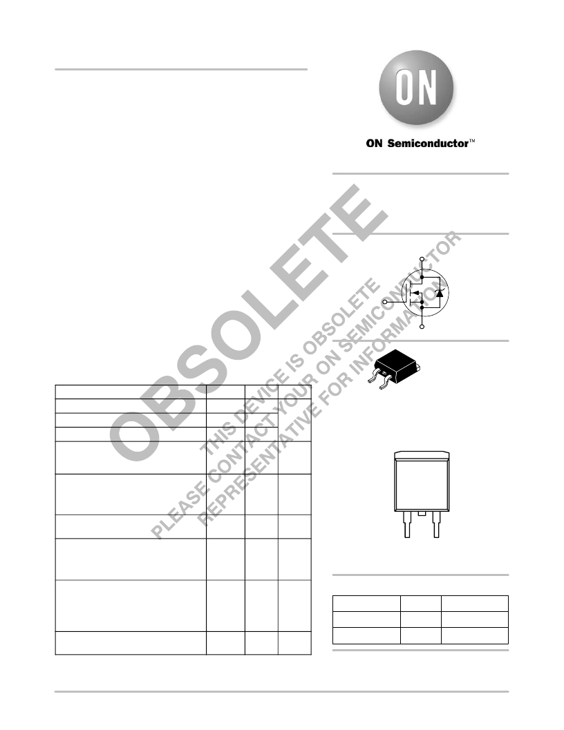
�D� 2� PAK�
�MAXIMUM� RATINGS� (T� C� =� 25� °� C� unless� otherwise� noted)�
�Rating� Symbol� Value�
�Unit�
�1�
�2�
�3�
�CASE� 418B�
�STYLE� 2�
�Drain� ?� to� ?� Source� Voltage�
�Drain� ?� to� ?� Gate� Voltage� (R� GS� =� 1.0� M� Ω� )�
�Gate� ?� to� ?� Source� Voltage� ?� Continuous�
�Drain� Current� ?� Continuous�
�Drain� Current� ?� Continuous� @� 100� °� C�
�Drain� Current� ?� Single� Pulse� (t� p� ≤� 10� μ� s)�
�Total� Power� Dissipation�
�Derate� above� 25� °� C�
�Total� Power� Dissipation� @� T� A� =� 25� °� C�
�(minimum� footprint,� FR� ?� 4� board)�
�V� DSS�
�V� DGR�
�V� GS�
�I� D�
�I� D�
�I� DM�
�P� D�
�50�
�50�
�±� 20�
�75�
�65�
�225�
�125�
�1.0�
�2.5�
�Volts�
�Amps�
�Watts�
�W/� °� C�
�Watts�
�MARKING� DIAGRAM�
�&� PIN� ASSIGNMENT�
�4�
�Drain�
�MTB75N05HD�
�YWW�
�Operating� and� Storage� Temperature�
�Range�
�T� J� ,� T� stg�
�?� 55� to�
�150�
�°� C�
�1�
�Gate�
�2�
�Drain�
�3�
�Source�
�Single� Pulse� Drain� ?� to� ?� Source� Avalanche�
�Energy� ?� Starting� T� J� =� 25� °� C�
�(V� DD� =� 25� V,� V� GS� =� 10� V,� Peak�
�I� L� =� 75� A,� L� =� 0.177� mH,� R� G� =� 25� Ω� )�
�Thermal� Resistance�
�?� Junction� to� Case�
�?� Junction� to� Ambient�
�?� Junction� to� Ambient� (minimum� foot-�
�print,� FR� ?� 4� board)�
�E� AS�
�R� θ� JC�
�R� θ� JA�
�R� θ� JA�
�500�
�1.0�
�62.5�
�50�
�mJ�
�°� C/W�
�MTB75N05HD� =� Device� Code�
�Y� =� Year�
�WW� =� Work� Week�
�ORDERING� INFORMATION�
�Device� Package� Shipping�
�MTB75N05HD� D� 2� PAK� 50� Units/Rail�
�Maximum� Temperature� for� Soldering�
�Purposes,� 1/8� ″� from� case� for� 10� s�
�T� L�
�260�
�°� C�
�MTB75N05HDT4�
�D� 2� PAK�
�800/Tape� &� Reel�
�Preferred� devices� are� recommended� choices� for� future� use�
�and� best� overall� value.�
�?� Semiconductor� Components� Industries,� LLC,� 2006�
�August,� 2006� ?� Rev.� 7�
�1�
�Publication� Order� Number:�
�MTB75N05HD/D�
�相关PDF资料 |
PDF描述 |
|---|---|
| MTCBA-C1-N3 | MODEM CDMA RS232 DUAL |
| MTCBA-C1-U-N2 | MODEM CDMA USB 800MHZ 1.9GHZ |
| MTCBA-C1X-N2-NAM | MODEM CDMA 800MHZ 1.9GHZ |
| MTCBA-G-EN-F4-ED-GB/IE | MODEM GPRS QUAD EU/UK ETH INTFC |
| MTCBA-G2 | MODEM GPRS CELLULAR SERIAL |
相关代理商/技术参数 |
参数描述 |
|---|---|
| MTB75N06 | 制造商:MOTOROLA 制造商全称:Motorola, Inc 功能描述:TMOS POWER FET 75 AMPERES 60 VOLTS |
| MTB75N06HD | 制造商:ON Semiconductor 功能描述:Trans MOSFET N-CH 60V 75A 3-Pin(2+Tab) D2PAK Rail |
| MTB7671 | 制造商:Megger 功能描述:METER TEST BOX |
| MTB-7PL80 | 制造商:ITT Interconnect Solutions 功能描述:MTB-7PL80 / 095262-0006 / MICRO |
| MTB-7SL80 | 制造商:ITT Interconnect Solutions 功能描述:MTB-7SL80 - Bulk |
发布紧急采购,3分钟左右您将得到回复。