- 您现在的位置:买卖IC网 > PDF目录187174 > MTD1N60ET4 (MOTOROLA INC) 1 A, 600 V, 8 ohm, N-CHANNEL, Si, POWER, MOSFET PDF资料下载
参数资料
| 型号: | MTD1N60ET4 |
| 厂商: | MOTOROLA INC |
| 元件分类: | JFETs |
| 英文描述: | 1 A, 600 V, 8 ohm, N-CHANNEL, Si, POWER, MOSFET |
| 封装: | CASE 369A-13, DPAK-3 |
| 文件页数: | 1/10页 |
| 文件大小: | 230K |
| 代理商: | MTD1N60ET4 |
NOT
RECOMMENDED
FOR
NEW
DESIGN
NOT
RECOMMENDED
FOR
NEW
DESIGN
1
Motorola TMOS Power MOSFET Transistor Device Data
Designer's Data Sheet
TMOS E-FET.
Power Field Effect Transistor
DPAK for Surface Mount
N–Channel Enhancement–Mode Silicon Gate
This high voltage MOSFET uses an advanced termination
scheme to provide enhanced voltage–blocking capability without
degrading performance over time. In addition this advanced TMOS
E–FET is designed to withstand high energy in the avalanche and
commutation modes. The new energy efficient design also offers a
drain–to–source diode with a fast recovery time. Designed for high
voltage, high speed switching applications in power supplies,
converters and PWM motor controls, these devices are particularly
well suited for bridge circuits where diode speed and commutating
safe operating areas are critical and offer additional safety margin
against unexpected voltage transients.
Robust High Voltage Termination
Avalanche Energy Specified
Source–to–Drain Diode Recovery Time Comparable to a Discrete
Fast Recovery Diode
Diode is Characterized for Use in Bridge Circuits
IDSS and VDS(on) Specified at Elevated Temperature
Surface Mount Package Available in 16 mm, 13–inch/2500
Unit Tape & Reel, Add T4 Suffix to Part Number
MAXIMUM RATINGS (TC = 25°C unless otherwise noted)
Rating
Symbol
Value
Unit
Drain–Source Voltage
VDSS
600
Vdc
Drain–Gate Voltage (RGS = 1.0 M)
VDGR
600
Vdc
Gate–Source Voltage — Continuous
— Non–Repetitive (tp ≤ 10 ms)
VGS
VGSM
± 20
± 40
Vdc
Vpk
Drain Current — Continuous
— Continuous @ 100
°C
— Single Pulse (tp ≤ 10 s)
ID
IDM
1.0
0.8
3.0
Adc
Apk
Total Power Dissipation
Derate above 25
°C
Total Power Dissipation @ TA = 25°C, when mounted to minimum recommended pad size
PD
40
0.32
1.75
Watts
W/
°C
Watts
Operating and Storage Temperature Range
TJ, Tstg
– 55 to 150
°C
Single Pulse Drain–to–Source Avalanche Energy — Starting TJ = 25°C
(VDD = 100 Vdc, VGS = 10 Vdc, IL = 3.0 Apk, L = 10 mH, RG = 25 )
EAS
45
mJ
Thermal Resistance — Junction to Case
— Junction to Ambient
— Junction to Ambient, when mounted to minimum recommended pad size
RθJC
RθJA
3.13
100
71.4
°C/W
Maximum Temperature for Soldering Purposes, 1/8
″ from case for 10 seconds
TL
260
°C
Designer’s Data for “Worst Case” Conditions — The Designer’s Data Sheet permits the design of most circuits entirely from the information presented. SOA Limit
curves — representing boundaries on device characteristics — are given to facilitate “worst case” design.
E–FET and Designer’s are trademarks of Motorola, Inc. TMOS is a registered trademark of Motorola, Inc.
Thermal Clad is a trademark of the Bergquist Company.
Preferred devices are Motorola recommended choices for future use and best overall value.
REV 1
Order this document
by MTD1N60E/D
MOTOROLA
SEMICONDUCTOR TECHNICAL DATA
Motorola, Inc. 1995
MTD1N60E
TMOS POWER FET
1.0 AMPERE
600 VOLTS
RDS(on) = 8.0 OHM
Motorola Preferred Device
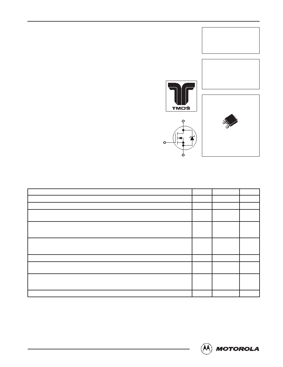
D
S
G
CASE 369A–13, Style 2
DPAK
相关PDF资料 |
PDF描述 |
|---|---|
| MTD1N80E | 1 A, 800 V, 12 ohm, N-CHANNEL, Si, POWER, MOSFET |
| MTD1N80ET4 | 1 A, 800 V, 12 ohm, N-CHANNEL, Si, POWER, MOSFET |
| MTD2955V1 | 12 A, 60 V, 0.23 ohm, P-CHANNEL, Si, POWER, MOSFET |
| MTD2955V1G | 12 A, 60 V, 0.23 ohm, P-CHANNEL, Si, POWER, MOSFET |
| MTD2N40ET4 | 2 A, 400 V, 3.5 ohm, N-CHANNEL, Si, POWER, MOSFET |
相关代理商/技术参数 |
参数描述 |
|---|---|
| MTD1N80E | 制造商:MOTOROLA 制造商全称:Motorola, Inc 功能描述:TMOS POWER FET 1.0 AMPERES 800 VOLTS RDS(on) = 12 OHM |
| MTD1P40ET4 | 制造商:Rochester Electronics LLC 功能描述:- Bulk |
| MTD1P50E | 制造商:MOTOROLA 制造商全称:Motorola, Inc 功能描述:TMOS POWER FET 1.0 AMPERES 500 VOLTS 15 OHM |
| MTD2001 | 制造商:SHINDENGEN 制造商全称:Shindengen Electric Mfg.Co.Ltd 功能描述:Stepping Motor Driver ICs |
| MTD2001-4101 | 功能描述:马达/运动/点火控制器和驱动器 VCEO=60 IO=1.5 PT=5 RoHS:否 制造商:STMicroelectronics 产品:Stepper Motor Controllers / Drivers 类型:2 Phase Stepper Motor Driver 工作电源电压:8 V to 45 V 电源电流:0.5 mA 工作温度:- 25 C to + 125 C 安装风格:SMD/SMT 封装 / 箱体:HTSSOP-28 封装:Tube |
发布紧急采购,3分钟左右您将得到回复。