- 您现在的位置:买卖IC网 > PDF目录98046 > MTD4N20E-1 (ON SEMICONDUCTOR) 4 A, 200 V, 1.2 ohm, N-CHANNEL, Si, POWER, MOSFET PDF资料下载
参数资料
| 型号: | MTD4N20E-1 |
| 厂商: | ON SEMICONDUCTOR |
| 元件分类: | JFETs |
| 英文描述: | 4 A, 200 V, 1.2 ohm, N-CHANNEL, Si, POWER, MOSFET |
| 封装: | CASE 369C, DPAK-3 |
| 文件页数: | 10/12页 |
| 文件大小: | 259K |
| 代理商: | MTD4N20E-1 |
MTD4N20E
http://onsemi.com
7
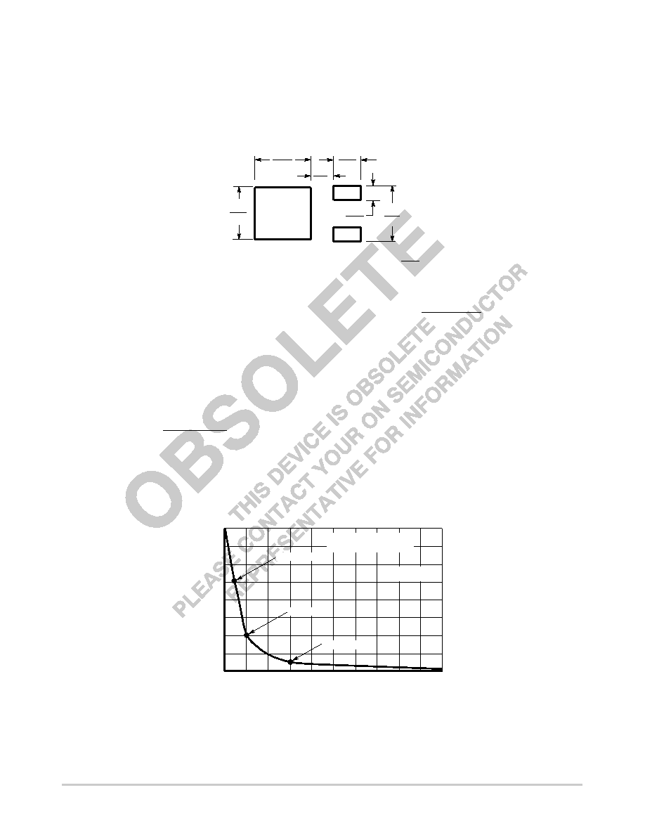
INFORMATION FOR USING THE DPAK SURFACE MOUNT PACKAGE
RECOMMENDED FOOTPRINT FOR SURFACE MOUNTED APPLICATIONS
Surface mount board layout is a critical portion of the
total design. The footprint for the semiconductor packages
must be the correct size to ensure proper solder connection
interface between the board and the package. With the
correct pad geometry, the packages will self align when
subjected to a solder reflow process.
5.80
0.228
2.58
0.101
1.6
0.063
6.20
0.244
3.0
0.118
6.172
0.243
mm
inches
SCALE 3:1
POWER DISSIPATION FOR A SURFACE MOUNT DEVICE
The power dissipation for a surface mount device is a
function of the drain pad size. These can vary from the
minimum pad size for soldering to a pad size given for
maximum power dissipation. Power dissipation for a
surface mount device is determined by TJ(max), the
maximum rated junction temperature of the die, RθJA, the
thermal resistance from the device junction to ambient, and
the operating temperature, TA. Using the values provided
on the data sheet, PD can be calculated as follows:
PD =
TJ(max) TA
RθJA
The values for the equation are found in the maximum
ratings table on the data sheet. Substituting these values
into the equation for an ambient temperature TA of 25°C,
one can calculate the power dissipation of the device. For a
DPAK device, PD is calculated as follows.
PD =
150
°C 25°C
71.4
°C/W
= 1.75 Watts
The 71.4
°C/W for the DPAK package assumes the use of
0.5 sq. in. source pad on a glass epoxy printed circuit board
to achieve a power dissipation of 1.75 Watts. There are
other alternatives to achieving higher power dissipation
from the surface mount packages. One is to increase the
area of the drain pad. By increasing the area of the drain
pad, the power dissipation can be increased. Although one
can almost double the power dissipation with this method,
one will be giving up area on the printed circuit board
which can defeat the purpose of using surface mount
technology. For example, a graph of RθJA versus drain pad
area is shown in Figure 15.
Figure 15. Thermal Resistance versus Drain Pad
Area for the DPAK Package (Typical)
1.75 Watts
Board Material = 0.0625″
G10/FR4, 2 oz Copper
80
100
60
40
20
10
8
6
4
2
0
3.0 Watts
5.0 Watts
TA = 25°C
A, AREA (SQUARE INCHES)
TO
AMBIENT
(
C/W)°
R
JA
,THERMAL
RESIST
ANCE,
JUNCTION
θ
Another alternative would be to use a ceramic substrate
or an aluminum core board such as Thermal Clad
t. Using
a board material such as Thermal Clad, an aluminum core
board, the power dissipation can be doubled using the same
footprint.
相关PDF资料 |
PDF描述 |
|---|---|
| MTD9N10ET4 | 9 A, 100 V, 0.25 ohm, N-CHANNEL, Si, POWER, MOSFET |
| MTD9N10E | 9 A, 100 V, 0.25 ohm, N-CHANNEL, Si, POWER, MOSFET |
| MTD9N10EG | 9 A, 100 V, 0.25 ohm, N-CHANNEL, Si, POWER, MOSFET |
| MTDF1C02HDR2 | 1700 mA, 20 V, 2 CHANNEL, N AND P-CHANNEL, Si, SMALL SIGNAL, MOSFET |
| MTDF1N02HDR2 | 1700 mA, 20 V, 2 CHANNEL, N-CHANNEL, Si, SMALL SIGNAL, MOSFET |
相关代理商/技术参数 |
参数描述 |
|---|---|
| MTD4N20ET4 | 制造商:Motorola 功能描述:4N20 MOT'96 SMT/REEL |
| MTD4P05 | 制造商:MOTOROLA 制造商全称:Motorola, Inc 功能描述:POWER FIELD EFFECT TRANSISTOR |
| MTD4P06 | 制造商:MOTOROLA 制造商全称:Motorola, Inc 功能描述:POWER FIELD EFFECT TRANSISTOR |
| MTD5010M | 制造商:MARKTECH 制造商全称:Marktech Corporate 功能描述:Ultra High Speed Photo Diode |
| MTD5010N | 功能描述:PHOTO DIODE 850NM DOME CLR TO-18 RoHS:是 类别:传感器,转换器 >> 光学 - 光电检测器 - 光电二极管 系列:- 标准包装:1 系列:- 波长:850nm 颜色 - 增强型:- 光谱范围:400nm ~ 1100nm 二极管类型:引脚 nm 下响应率:0.62 A/W @ 850nm 响应时间:5ns 电压 - (Vr)(最大):50V 电流 - 暗(标准):1nA 有效面积:1mm² 视角:150° 工作温度:-40°C ~ 100°C 封装/外壳:径向,5mm 直径(T 1 3/4) 其它名称:475-2649-6 |
发布紧急采购,3分钟左右您将得到回复。