- 您现在的位置:买卖IC网 > PDF目录96092 > MTD4N20E-T4 (MOTOROLA INC) 4 A, 200 V, 1.2 ohm, N-CHANNEL, Si, POWER, MOSFET PDF资料下载
参数资料
| 型号: | MTD4N20E-T4 |
| 厂商: | MOTOROLA INC |
| 元件分类: | JFETs |
| 英文描述: | 4 A, 200 V, 1.2 ohm, N-CHANNEL, Si, POWER, MOSFET |
| 文件页数: | 1/10页 |
| 文件大小: | 268K |
| 代理商: | MTD4N20E-T4 |
1
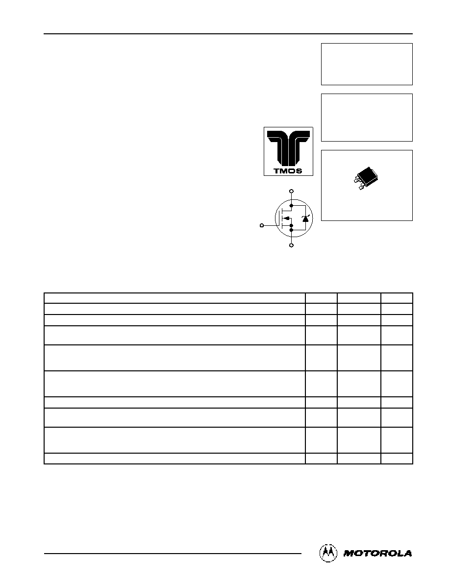
Motorola TMOS Power MOSFET Transistor Device Data
Designer's Data Sheet
TMOS E-FET.
Power Field Effect Transistor
DPAK for Surface Mount
N–Channel Enhancement–Mode Silicon Gate
This advanced TMOS E–FET is designed to withstand high
energy in the avalanche and commutation modes. The new energy
efficient design also offers a drain–to–source diode with a fast
recovery time. Designed for low voltage, high speed switching
applications in power supplies, converters and PWM motor
controls, these devices are particularly well suited for bridge circuits
where diode speed and commutating safe operating areas are
critical and offer additional safety margin against unexpected
voltage transients.
Avalanche Energy Specified
Source–to–Drain Diode Recovery Time Comparable to a
Discrete Fast Recovery Diode
Diode is Characterized for Use in Bridge Circuits
IDSS and VDS(on) Specified at Elevated Temperature
Surface Mount Package Available in 16 mm, 13–inch/2500
Unit Tape & Reel, Add –T4 Suffix to Part Number
MAXIMUM RATINGS (TC = 25°C unless otherwise noted)
Rating
Symbol
Value
Unit
Drain–Source Voltage
VDSS
200
Vdc
Drain–Gate Voltage (RGS = 1.0 M)
VDGR
200
Vdc
Gate–Source Voltage — Continuous
— Non–repetitive (tp ≤ 10 ms)
VGS
VGSM
± 20
± 40
Vdc
Vpk
Drain Current — Continuous
Drain Current — Continuous @ 100
°C
Drain Current — Single Pulse (tp ≤ 10 s)
ID
IDM
4.0
2.6
12
Adc
Apk
Total Power Dissipation @ TC = 25°C
Derate above 25
°C
Total Power Dissipation @ TA = 25°C, when mounted to minimum recommended pad size
PD
40
0.32
1.75
Watts
W/
°C
Watts
Operating and Storage Temperature Range
TJ, Tstg
– 55 to 150
°C
Single Pulse Drain–to–Source Avalanche Energy — Starting TJ = 25°C
(VDD = 80 Vdc, VGS = 10 Vdc, IL = 4.0 Apk, L = 10 mH, RG = 25 )
EAS
80
mJ
Thermal Resistance — Junction to Case
Thermal Resistance — Junction to Ambient
Thermal Resistance — Junction to Ambient, when mounted to minimum recommended pad size
R
θJC
R
θJA
R
θJA
3.13
100
71.4
°C/W
Maximum Temperature for Soldering Purposes, 1/8
″ from case for 10 seconds
TL
260
°C
Designer’s Data for “Worst Case” Conditions — The Designer’s Data Sheet permits the design of most circuits entirely from the information presented. SOA Limit
curves — representing boundaries on device characteristics — are given to facilitate “worst case” design.
E–FET and Designer’s are trademarks of Motorola, Inc. TMOS is a registered trademark of Motorola, Inc.
Thermal Clad is a trademark of the Bergquist Company.
Preferred devices are Motorola recommended choices for future use and best overall value.
REV 1
Order this document
by MTD4N20E/D
MOTOROLA
SEMICONDUCTOR TECHNICAL DATA
Motorola, Inc. 1995
MTD4N20E
TMOS POWER FET
4.0 AMPERES
200 VOLTS
RDS(on) = 1.2 OHM
Motorola Preferred Device
D
S
G
CASE 369A–13, Style 2
DPAK
相关PDF资料 |
PDF描述 |
|---|---|
| MTD5N25E-T4 | 5 A, 250 V, 1 ohm, N-CHANNEL, Si, POWER, MOSFET |
| MTD5P06ET4 | 5 A, 60 V, 0.55 ohm, P-CHANNEL, Si, POWER, MOSFET |
| MTD5P06V-1 | 5 A, 60 V, 0.45 ohm, P-CHANNEL, Si, POWER, MOSFET |
| MTD5P06V1 | 5 A, 60 V, 0.45 ohm, P-CHANNEL, Si, POWER, MOSFET |
| MTD6N08 | 6 A, 80 V, 0.25 ohm, N-CHANNEL, Si, POWER, MOSFET, TO-252 |
相关代理商/技术参数 |
参数描述 |
|---|---|
| MTD4P05 | 制造商:MOTOROLA 制造商全称:Motorola, Inc 功能描述:POWER FIELD EFFECT TRANSISTOR |
| MTD4P06 | 制造商:MOTOROLA 制造商全称:Motorola, Inc 功能描述:POWER FIELD EFFECT TRANSISTOR |
| MTD5010M | 制造商:MARKTECH 制造商全称:Marktech Corporate 功能描述:Ultra High Speed Photo Diode |
| MTD5010N | 功能描述:PHOTO DIODE 850NM DOME CLR TO-18 RoHS:是 类别:传感器,转换器 >> 光学 - 光电检测器 - 光电二极管 系列:- 标准包装:1 系列:- 波长:850nm 颜色 - 增强型:- 光谱范围:400nm ~ 1100nm 二极管类型:引脚 nm 下响应率:0.62 A/W @ 850nm 响应时间:5ns 电压 - (Vr)(最大):50V 电流 - 暗(标准):1nA 有效面积:1mm² 视角:150° 工作温度:-40°C ~ 100°C 封装/外壳:径向,5mm 直径(T 1 3/4) 其它名称:475-2649-6 |
| MTD5010N-DIG | 制造商:Marktech Optoelectronics 功能描述:PHOTO DIODE 850NM DOME CLR TO-18 |
发布紧急采购,3分钟左右您将得到回复。