- 您现在的位置:买卖IC网 > PDF目录96092 > MTD5P06V1 (ON SEMICONDUCTOR) 5 A, 60 V, 0.45 ohm, P-CHANNEL, Si, POWER, MOSFET PDF资料下载
参数资料
| 型号: | MTD5P06V1 |
| 厂商: | ON SEMICONDUCTOR |
| 元件分类: | JFETs |
| 英文描述: | 5 A, 60 V, 0.45 ohm, P-CHANNEL, Si, POWER, MOSFET |
| 封装: | CASE 369D-01, DPAK-3 |
| 文件页数: | 1/8页 |
| 文件大小: | 150K |
| 代理商: | MTD5P06V1 |
Semiconductor Components Industries, LLC, 2006
March, 2006 Rev. 5
1
Publication Order Number:
MTD5P06V/D
MTD5P06V
Preferred Device
Power MOSFET
5 Amps, 60 Volts PChannel DPAK
This Power MOSFET is designed to withstand high energy in the
avalanche and commutation modes. Designed for low voltage, high
speed switching applications in power supplies, converters and power
motor controls, these devices are particularly well suited for bridge
circuits where diode speed and commutating safe operating areas are
critical and offer additional safety margin against unexpected voltage
transients.
Avalanche Energy Specified
IDSS and VDS(on) Specified at Elevated Temperature
w These devices are available in Pbfree package(s). Specifications herein
apply to both standard and Pbfree devices. Please see our website at
www.onsemi.com for specific Pbfree orderable part numbers, or
contact your local ON Semiconductor sales office or representative.
MAXIMUM RATINGS (TC = 25°C unless otherwise noted)
Rating
Symbol
Value
Unit
DraintoSource Voltage
VDSS
60
Vdc
DraintoGate Voltage (RGS = 1.0 MΩ)
VDGR
60
Vdc
GatetoSource Voltage
Continuous
Nonrepetitive (tp ≤ 10 ms)
VGS
VGSM
± 15
± 25
Vdc
Vpk
Drain Current Continuous @ 25°C
Drain Current Continuous @ 100°C
Drain Current Single Pulse (tp ≤ 10 μs)
ID
IDM
5
4
18
Adc
Apk
Total Power Dissipation @ 25°C
Derate above 25°C
Total Power Dissipation @ TA = 25°C
(Note 2)
PD
40
0.27
2.1
Watts
W/°C
Watts
Operating and Storage Temperature Range
TJ, Tstg
55 to
175
°C
Single Pulse DraintoSource Avalanche
Energy Starting TJ = 25°C
(VDD = 25 Vdc, VGS = 10 Vdc, Peak
IL = 5 Apk, L = 10 mH, RG = 25 Ω)
EAS
125
mJ
Thermal Resistance
JunctiontoCase
JunctiontoAmbient (Note 1)
JunctiontoAmbient (Note 2)
RθJC
RθJA
3.75
100
71.4
°C/W
Maximum Lead Temperature for Soldering
Purposes, 1/8″ from Case for 10 sec
TL
260
°C
Stresses exceeding Maximum Ratings may damage the device. Maximum
Ratings are stress ratings only. Functional operation above the Recommended
Operating Conditions is not implied. Extended exposure to stresses above the
Recommended Operating Conditions may affect device reliability.
1. When surface mounted to an FR4 board using the minimum
recommended pad size.
2. When surface mounted to an FR4 board using the 0.5 sq in drain pad size.
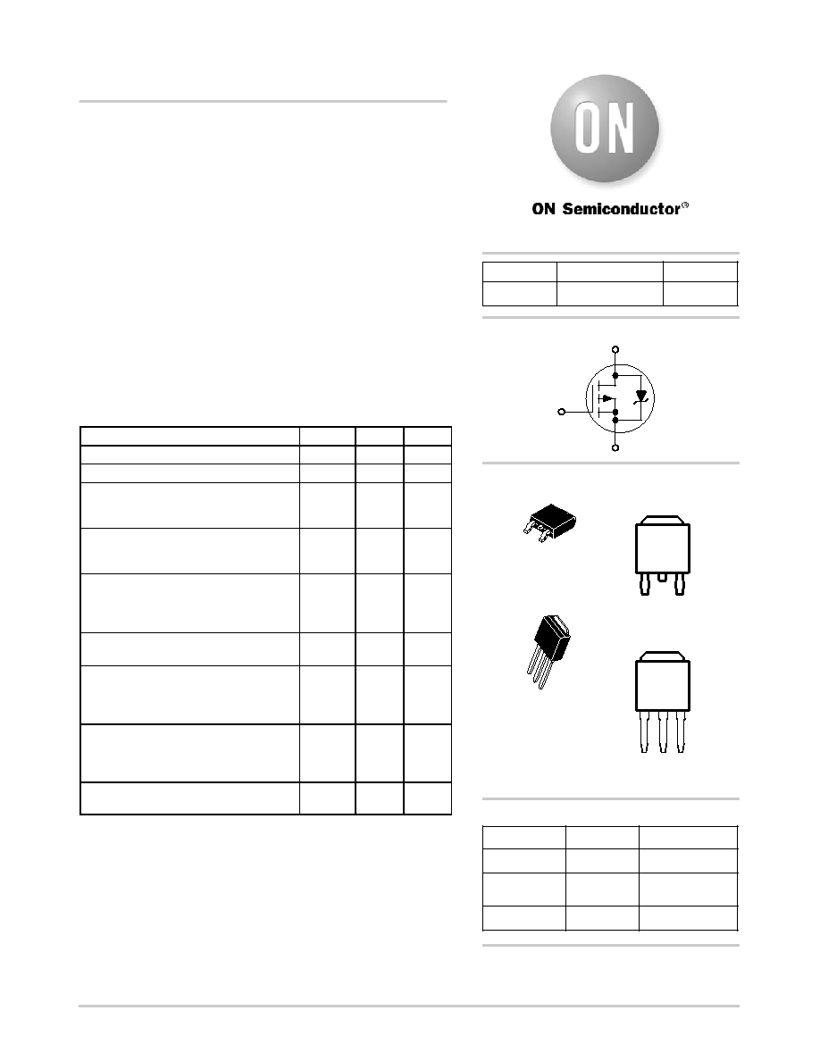
D
S
G
PChannel
Preferred devices are recommended choices for future use
and best overall value.
http://onsemi.com
60 V
340 mW
RDS(on) TYP
5.0 A
ID MAX
V(BR)DSS
1
Gate
3
Source
2
Drain
4
Drain
DPAK
CASE 369C
Style 2
MARKING DIAGRAMS
5P06V
Device Code
Y
= Year
WW
= Work Week
1 2
3
4
1
Gate
3
Source
2
Drain
4
Drain
DPAK
CASE 369D
Style 2
1
2
3
4
Device
Package
Shipping
ORDERING INFORMATION
MTD5P06V
DPAK
75 Units/Rail
MTD5P06V1
DPAK
Straight Lead
75 Units/Rail
MTD5P06VT4
DPAK
2500 Tape & Reel
YWW
5P06V
YWW
5P06V
相关PDF资料 |
PDF描述 |
|---|---|
| MTD6N08 | 6 A, 80 V, 0.25 ohm, N-CHANNEL, Si, POWER, MOSFET, TO-252 |
| MTD6N08-1 | 6 A, 80 V, 0.25 ohm, N-CHANNEL, Si, POWER, MOSFET, TO-251 |
| MTD6N151 | 6 A, 150 V, 0.3 ohm, N-CHANNEL, Si, POWER, MOSFET |
| MTD6N15T4 | 6 A, 150 V, 0.3 ohm, N-CHANNEL, Si, POWER, MOSFET |
| MTD6N20E1 | 6 A, 200 V, 0.7 ohm, N-CHANNEL, Si, POWER, MOSFET |
相关代理商/技术参数 |
参数描述 |
|---|---|
| MTD5P06VT4 | 功能描述:MOSFET 60V 5A P-Channel RoHS:否 制造商:STMicroelectronics 晶体管极性:N-Channel 汲极/源极击穿电压:650 V 闸/源击穿电压:25 V 漏极连续电流:130 A 电阻汲极/源极 RDS(导通):0.014 Ohms 配置:Single 最大工作温度: 安装风格:Through Hole 封装 / 箱体:Max247 封装:Tube |
| MTD5P06VT4G | 功能描述:MOSFET PFET DPAK 60V 5A 450mOhm RoHS:否 制造商:STMicroelectronics 晶体管极性:N-Channel 汲极/源极击穿电压:650 V 闸/源击穿电压:25 V 漏极连续电流:130 A 电阻汲极/源极 RDS(导通):0.014 Ohms 配置:Single 最大工作温度: 安装风格:Through Hole 封装 / 箱体:Max247 封装:Tube |
| MTD5P06VT4G | 制造商:ON Semiconductor 功能描述:MOSFET |
| MTD5P06VT4GV | 功能描述:MOSFET Single P-Ch 60V 5A RoHS:否 制造商:STMicroelectronics 晶体管极性:N-Channel 汲极/源极击穿电压:650 V 闸/源击穿电压:25 V 漏极连续电流:130 A 电阻汲极/源极 RDS(导通):0.014 Ohms 配置:Single 最大工作温度: 安装风格:Through Hole 封装 / 箱体:Max247 封装:Tube |
| MTD6000PT | 制造商:MARKTECH 制造商全称:Marktech Corporate 功能描述:Photo Transistor |
发布紧急采购,3分钟左右您将得到回复。