- 您现在的位置:买卖IC网 > PDF目录18673 > MTD5P06VT4G (ON Semiconductor)MOSFET P-CH 60V 5A DPAK PDF资料下载
参数资料
| 型号: | MTD5P06VT4G |
| 厂商: | ON Semiconductor |
| 文件页数: | 5/7页 |
| 文件大小: | 0K |
| 描述: | MOSFET P-CH 60V 5A DPAK |
| 产品目录绘图: | MOSFET DPAK Pkg |
| 标准包装: | 10 |
| FET 型: | MOSFET P 通道,金属氧化物 |
| FET 特点: | 标准 |
| 漏极至源极电压(Vdss): | 60V |
| 电流 - 连续漏极(Id) @ 25° C: | 5A |
| 开态Rds(最大)@ Id, Vgs @ 25° C: | 450 毫欧 @ 2.5A,10V |
| Id 时的 Vgs(th)(最大): | 4V @ 250µA |
| 闸电荷(Qg) @ Vgs: | 20nC @ 10V |
| 输入电容 (Ciss) @ Vds: | 510pF @ 25V |
| 功率 - 最大: | 40W |
| 安装类型: | 表面贴装 |
| 封装/外壳: | TO-252-3,DPak(2 引线+接片),SC-63 |
| 供应商设备封装: | DPAK-3 |
| 包装: | 标准包装 |
| 产品目录页面: | 1558 (CN2011-ZH PDF) |
| 其它名称: | MTD5P06VT4GOSDKR |
�� �
�
�MTD5P06V�
�10�
�9�
�QT�
�V� GS�
�60�
�54�
�100�
�T� J� =� 25� °� C�
�I� D� =� 5� A�
�8�
�48�
�V� DD� =� 30� V�
�7�
�Q1�
�Q2�
�42�
�V� GS� =� 10� V�
�t� r�
�6�
�36�
�t� d(off)�
�5�
�30�
�10�
�t� f�
�t� d(on)�
�4�
�3�
�24�
�18�
�2�
�1�
�Q3�
�V� DS�
�T� J� =� 25� °� C�
�I� D� =� 5� A�
�12�
�6�
�0�
�0�
�2�
�4�
�6�
�8�
�10�
�12�
�0�
�14�
�1�
�1�
�10�
�100�
�Q� g� ,� TOTAL� GATE� CHARGE� (nC)�
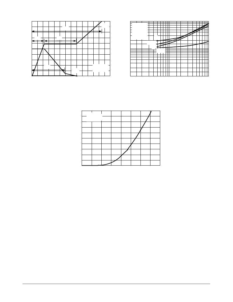
�Figure� 8.� Gate?To?Source� and� Drain?To?Source�
�Voltage� versus� Total� Charge�
�R� G� ,� GATE� RESISTANCE� (OHMS)�
�Figure� 9.� Resistive� Switching� Time�
�Variation� versus� Gate� Resistance�
�DRAIN?TO?SOURCE� DIODE� CHARACTERISTICS�
�5�
�4.5�
�4�
�3.5�
�3�
�2.5�
�2�
�1.5�
�1�
�0.5�
�T� J� =� 25� °� C�
�V� GS� =� 0� V�
�0�
�0.2�
�0.4�
�0.6�
�0.8�
�1�
�1.2�
�1.4�
�1.6�
�1.8�
�V� SD� ,� SOURCE?TO?DRAIN� VOLTAGE� (VOLTS)�
�Figure� 10.� Diode� Forward� Voltage� versus� Current�
�SAFE� OPERATING� AREA�
�The� Forward� Biased� Safe� Operating� Area� curves� define� the�
�maximum� simultaneous� drain?to?source� voltage� and� drain�
�current� that� a� transistor� can� handle� safely� when� it� is� forward�
�biased.� Curves� are� based� upon� maximum� peak� junction�
�temperature� and� a� case� temperature� (T� C� )� of� 25� °� C.� Peak�
�repetitive� pulsed� power� limits� are� determined� by� using� the�
�thermal� response� data� in� conjunction� with� the� procedures�
�discussed� in� AN569,� “Transient� Thermal� Resistance?General�
�Data� and� Its� Use.”�
�Switching� between� the� off?state� and� the� on?state� may�
�traverse� any� load� line� provided� neither� rated� peak� current�
�(I� DM� )� nor� rated� voltage� (V� DSS� )� is� exceeded� and� the�
�transition� time� (t� r� ,t� f� )� do� not� exceed� 10� m� s.� In� addition� the� total�
�power� averaged� over� a� complete� switching� cycle� must� not�
�exceed� (T� J(MAX)� ?� T� C� )/(R� q� JC� ).�
�A� Power� MOSFET� designated� E?FET� can� be� safely� used�
�reliable� operation,� the� stored� energy� from� circuit� inductance�
�dissipated� in� the� transistor� while� in� avalanche� must� be� less�
�than� the� rated� limit� and� adjusted� for� operating� conditions�
�differing� from� those� specified.� Although� industry� practice� is�
�to� rate� in� terms� of� energy,� avalanche� energy� capability� is� not�
�a� constant.� The� energy� rating� decreases� non?linearly� with� an�
�increase� of� peak� current� in� avalanche� and� peak� junction�
�temperature.�
�Although� many� E?FETs� can� withstand� the� stress� of�
�drain?to?source� avalanche� at� currents� up� to� rated� pulsed�
�current� (I� DM� ),� the� energy� rating� is� specified� at� rated�
�continuous� current� (I� D� ),� in� accordance� with� industry�
�custom.� The� energy� rating� must� be� derated� for� temperature�
�as� shown� in� the� accompanying� graph� (Figure� 12).� Maximum�
�energy� at� currents� below� rated� continuous� I� D� can� safely� be�
�assumed� to� equal� the� values� indicated.�
�in� switching� circuits� with� unclamped� inductive� loads.� For�
�http://onsemi.com�
�5�
�相关PDF资料 |
PDF描述 |
|---|---|
| XMLHVW-Q0-0000-0000LT353 | LED XM-L HIGH VOLTAGE WHITE |
| IXFH6N100 | MOSFET N-CH 1KV 6A TO-247AD |
| 184S72 | CABLE SGL-END R/A FMAL 4POS 6' |
| 674S4SS6L | CABLE STR 4POS FEMALE/FEMALE 6M |
| OPB910W55Z | SWITCH SLOTTED OPTICAL WIDE GAP |
相关代理商/技术参数 |
参数描述 |
|---|---|
| MTD5P06VT4G | 制造商:ON Semiconductor 功能描述:MOSFET |
| MTD5P06VT4GV | 功能描述:MOSFET Single P-Ch 60V 5A RoHS:否 制造商:STMicroelectronics 晶体管极性:N-Channel 汲极/源极击穿电压:650 V 闸/源击穿电压:25 V 漏极连续电流:130 A 电阻汲极/源极 RDS(导通):0.014 Ohms 配置:Single 最大工作温度: 安装风格:Through Hole 封装 / 箱体:Max247 封装:Tube |
| MTD6000PT | 制造商:MARKTECH 制造商全称:Marktech Corporate 功能描述:Photo Transistor |
| MTD6000PTT | 制造商:MARKTECH 制造商全称:Marktech Corporate 功能描述:Peak Sensitivity Wavelength: 880nm |
| MTD6000PT-T | 功能描述:PHOTOTRANS 880NM PIGTAIL DOME RoHS:是 类别:传感器,转换器 >> 光学 - 光电检测器 - 光电晶体管 系列:- 标准包装:1,200 系列:- 电压 - 集电极发射极击穿(最大):30V 电流 - 集电极 (Ic)(最大):1mA 电流 - 暗 (Id)(最大):100nA 波长:880nm 视角:24° 功率 - 最大:100mW 安装类型:通孔 方向:顶视图 封装/外壳:径向 |
发布紧急采购,3分钟左右您将得到回复。