- 您现在的位置:买卖IC网 > Datasheet目录480 > MTD6N20ET4 (ON Semiconductor)MOSFET N-CH 200V 6A DPAK Datasheet资料下载
参数资料
| 型号: | MTD6N20ET4 |
| 厂商: | ON Semiconductor |
| 文件页数: | 1/7页 |
| 文件大小: | 0K |
| 描述: | MOSFET N-CH 200V 6A DPAK |
| 产品变化通告: | Product Obsolescence 21/Jan/2010 |
| 标准包装: | 10 |
| FET 型: | MOSFET N 通道,金属氧化物 |
| FET 特点: | 标准 |
| 漏极至源极电压(Vdss): | 200V |
| 电流 - 连续漏极(Id) @ 25° C: | 6A |
| 开态Rds(最大)@ Id, Vgs @ 25° C: | 700 毫欧 @ 3A,10V |
| Id 时的 Vgs(th)(最大): | 4V @ 250µA |
| 闸电荷(Qg) @ Vgs: | 21nC @ 10V |
| 输入电容 (Ciss) @ Vds: | 480pF @ 25V |
| 功率 - 最大: | 1.75W |
| 安装类型: | 表面贴装 |
| 封装/外壳: | TO-252-3,DPak(2 引线+接片),SC-63 |
| 供应商设备封装: | DPAK-3 |
| 包装: | 标准包装 |
| 其它名称: | MTD6N20ET4OSDKR |
�� �
�
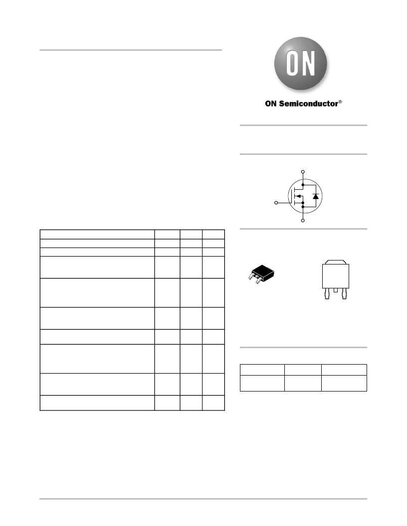
�MTD6N20E�
�Power� MOSFET�
�6� A,� 200� V,� N� ?� Channel� DPAK�
�This� advanced� Power� MOSFET� is� designed� to� withstand� high�
�energy� in� the� avalanche� and� commutation� modes.� The� new� energy�
�efficient� design� also� offers� a� drain� ?� to� ?� source� diode� with� a� fast�
�recovery� time.� Designed� for� low� voltage,� high� speed� switching�
�applications� in� power� supplies,� converters� and� PWM� motor� controls,�
�these� devices� are� particularly� well� suited� for� bridge� circuits� where�
�diode� speed� and� commutating� safe� operating� areas� are� critical� and�
�offer� additional� safety� margin� against� unexpected� voltage� transients.�
�http://onsemi.com�
�6� AMPERES,� 200� VOLTS�
�R� DS(on)� =� 460� m� W�
�Features�
�?� Avalanche� Energy� Specified�
�?� Source� ?� to� ?� Drain� Diode� Recovery� Time� Comparable� to� a�
�Discrete� Fast� Recovery� Diode�
�?� Diode� is� Characterized� for� Use� in� Bridge� Circuits�
�?� I� DSS� and� V� DS(on)� Specified� at� Elevated� Temperature�
�?� These� Devices� are� Pb� ?� Free� and� are� RoHS� Compliant�
�MAXIMUM� RATINGS� (T� C� =� 25� °� C� unless� otherwise� noted)�
�G�
�N� ?� Channel�
�D�
�S�
�Rating�
�Drain� ?� to� ?� Source� Voltage�
�Drain� ?� to� ?� Gate� Voltage� (R� GS� =� 1.0� M� W� )�
�Gate� ?� to� ?� Source� Voltage�
�?� Continuous�
�?� Non� ?� repetitive� (t� p� ≤� 10� ms)�
�Drain� Current�
�?� Continuous�
�?� Continuous� @� 100� °� C�
�?� Single� Pulse� (t� p� ≤� 10� m� s)�
�Symbol�
�V� DSS�
�V� DGR�
�V� GS�
�V� GSM�
�I� D�
�I� D�
�I� DM�
�Value�
�200�
�200�
�±� 20�
�±� 40�
�6.0�
�3.8�
�18�
�Unit�
�Vdc�
�Vdc�
�Vdc�
�Vpk�
�Adc�
�Apk�
�1� 2�
�3�
�4�
�DPAK�
�CASE� 369C�
�STYLE� 2�
�MARKING�
�DIAGRAMS�
�4 Drai� n�
�1� 2� 3�
�Gate� Drain� Source�
�Total� Power� Dissipation�
�Derate� above� 25� °� C�
�Total� Power� Dissipation� @� T� A� =� 25� °� C� (Note� 2)�
�Operating� and� Storage� Temperature� Range�
�P� D�
�T� J� ,� T� stg�
�50�
�0.4�
�1.75�
�?� 55� to�
�150�
�W�
�W/� °� C�
�W�
�°� C�
�6N20E�
�Y�
�WW�
�G�
�Device� Code�
�=� Year�
�=� Work� Week�
�=� Pb� ?� Free� Package�
�Single� Pulse� Drain� ?� to� ?� Source� Avalanche�
�Energy� ?� Starting� T� J� =� 25� °� C�
�(V� DD� =� 80� Vdc,� V� GS� =� 10� Vdc,�
�I� L� =� 6.0� Apk,� L� =� 3.0� mH,� R� G� =� 25� W� )�
�E� AS�
�54�
�mJ�
�ORDERING� INFORMATION�
�Device� Package� Shipping� ?�
�?� Junction� ?� to� ?� Ambient� (Note� 2)�
�Thermal� Resistance� ?� Junction� ?� to� ?� Case� R� q� JC� 2.50� °� C/W�
�?� Junction� ?� to� ?� Ambient� (Note� 1)� R� q� JA� 100�
�R� q� JA� 71.4�
�Maximum� Temperature� for� Soldering� T� L� 260� °� C�
�Purposes,� 1/8� ″� from� case� for� 10� secs�
�Stresses� exceeding� Maximum� Ratings� may� damage� the� device.� Maximum�
�Ratings� are� stress� ratings� only.� Functional� operation� above� the� Recommended�
�Operating� Conditions� is� not� implied.� Extended� exposure� to� stresses� above� the�
�Recommended� Operating� Conditions� may� affect� device� reliability.�
�1.� When� surface� mounted� to� an� FR4� board� using� the� minimum� recommended�
�pad� size.�
�2.� When� surface� mounted� to� an� FR4� board� using� the� 0.5� sq.� in.� drain� pad� size.�
�*For� additional� information� on� our� Pb� ?� Free� strategy� and� soldering� details,�
�please� download� the� ON� Semiconductor� Soldering� and� Mounting� Techniques�
�Reference� Manual,� SOLDERRM/D.�
�MTD6N20ET4G� DPAK� 2500� /� Tape� &�
�(Pb� ?� Free)� Reel�
�?For� information� on� tape� and� reel� specifications,�
�including� part� orientation� and� tape� sizes,� please�
�refer� to� our� Tape� and� Reel� Packaging� Specification�
�Brochure,� BRD8011/D.�
�?� Semiconductor� Components� Industries,� LLC,� 2013�
�April,� 2013� ?� Rev.� 6�
�1�
�Publication� Order� Number:�
�MTD6N20E/D�
�相关PDF资料 |
PDF描述 |
|---|---|
| MTD6P10E | MOSFET P-CH 100V 6A DPAK |
| MTD8000N4-T | PHOTOTRANS 880NM DOME CLR TO-18 |
| MTD8600N-T | PHOTOTRANS 880NM DOME CLR TO-18 |
| MTD8600N4-T | PHOTOTRANS 880NM DOME CLR TO-18 |
| MTD8600T-T | PHOTOTRANS 880NM FLAT CLR TO-18 |
相关代理商/技术参数 |
参数描述 |
|---|---|
| MTD6N20ET4G | 功能描述:MOSFET NFET DPAK 200V 6A 700mOhm RoHS:否 制造商:STMicroelectronics 晶体管极性:N-Channel 汲极/源极击穿电压:650 V 闸/源击穿电压:25 V 漏极连续电流:130 A 电阻汲极/源极 RDS(导通):0.014 Ohms 配置:Single 最大工作温度: 安装风格:Through Hole 封装 / 箱体:Max247 封装:Tube |
| MTD6N20ET5G | 功能描述:MOSFET NFET DPAK 200V 6A 700MO RoHS:否 制造商:STMicroelectronics 晶体管极性:N-Channel 汲极/源极击穿电压:650 V 闸/源击穿电压:25 V 漏极连续电流:130 A 电阻汲极/源极 RDS(导通):0.014 Ohms 配置:Single 最大工作温度: 安装风格:Through Hole 封装 / 箱体:Max247 封装:Tube |
| MTD6P10E | 功能描述:MOSFET P-CH 100V 6A DPAK RoHS:否 类别:分离式半导体产品 >> FET - 单 系列:- 标准包装:1,000 系列:MESH OVERLAY™ FET 型:MOSFET N 通道,金属氧化物 FET 特点:逻辑电平门 漏极至源极电压(Vdss):200V 电流 - 连续漏极(Id) @ 25° C:18A 开态Rds(最大)@ Id, Vgs @ 25° C:180 毫欧 @ 9A,10V Id 时的 Vgs(th)(最大):4V @ 250µA 闸电荷(Qg) @ Vgs:72nC @ 10V 输入电容 (Ciss) @ Vds:1560pF @ 25V 功率 - 最大:40W 安装类型:通孔 封装/外壳:TO-220-3 整包 供应商设备封装:TO-220FP 包装:管件 |
| MTD6P10ET4 | 制造商:ON Semiconductor 功能描述:Trans MOSFET P-CH 100V 6A 3-Pin(2+Tab) DPAK T/R |
| MTD7030 | 制造商:MARKTECH 制造商全称:Marktech Corporate 功能描述:PHOTO DIODE |
发布紧急采购,3分钟左右您将得到回复。