- 您现在的位置:买卖IC网 > PDF目录98049 > MUN5115T3 (MOTOROLA INC) 100 mA, 50 V, PNP, Si, SMALL SIGNAL TRANSISTOR PDF资料下载
参数资料
| 型号: | MUN5115T3 |
| 厂商: | MOTOROLA INC |
| 元件分类: | 小信号晶体管 |
| 英文描述: | 100 mA, 50 V, PNP, Si, SMALL SIGNAL TRANSISTOR |
| 封装: | SC-70, 3 PIN |
| 文件页数: | 11/12页 |
| 文件大小: | 196K |
| 代理商: | MUN5115T3 |
MUN5111T1 SERIES
http://onsemi.com
8
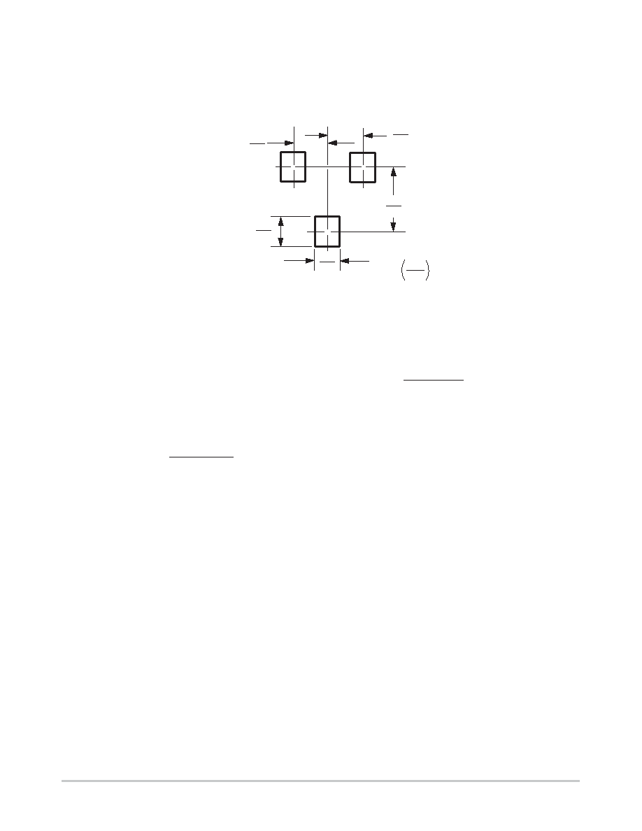
MINIMUM RECOMMENDED FOOTPRINTS FOR SURFACE MOUNTED APPLICATIONS
Surface mount board layout is a critical portion of the
total design. The footprint for the semiconductor packages
must be the correct size to insure proper solder connection
interface between the board and the package. With the
correct pad geometry, the packages will self align when
subjected to a solder reflow process.
mm
inches
0.035
0.9
0.075
0.7
1.9
0.028
0.65
0.025
0.65
0.025
SC–70/SOT–323 POWER DISSIPATION
The power dissipation of the SC–70/SOT–323 is a
function of the pad size. This can vary from the minimum
pad size for soldering to the pad size given for maximum
power dissipation. Power dissipation for a surface mount
device is determined by TJ(max), the maximum rated
junction temperature of the die, RθJA, the thermal
resistance from the device junction to ambient; and the
operating temperature, TA. Using the values provided on
the data sheet, PD can be calculated as follows:
PD =
TJ(max) – TA
RθJA
The values for the equation are found in the maximum
ratings table on the data sheet. Substituting these values
into the equation for an ambient temperature TA of 25°C,
one can calculate the power dissipation of the device which
in this case is 150 milliwatts.
PD =
150
°C – 25°C
= 150 milliwatts
833
°C/W
The 833
°C/W assumes the use of the recommended
footprint on a glass epoxy printed circuit board to achieve a
power dissipation of 150 milliwatts. Another alternative
would be to use a ceramic substrate or an aluminum core
board such as Thermal Clad
. Using a board material such
as Thermal Clad, a power dissipation of 300 milliwatts can
be achieved using the same footprint.
SOLDERING PRECAUTIONS
The melting temperature of solder is higher than the rated
temperature of the device. When the entire device is heated
to a high temperature, failure to complete soldering within
a short time could result in device failure. Therefore, the
following items should always be observed in order to
minimize the thermal stress to which the devices are
subjected.
Always preheat the device.
The delta temperature between the preheat and
soldering should be 100
°C or less.*
When preheating and soldering, the temperature of the
leads and the case must not exceed the maximum
temperature ratings as shown on the data sheet. When
using infrared heating with the reflow soldering
method, the difference should be a maximum of 10
°C.
The soldering temperature and time should not exceed
260
°C for more than 10 seconds.
When shifting from preheating to soldering, the
maximum temperature gradient should be 5
°C or less.
After soldering has been completed, the device should
be allowed to cool naturally for at least three minutes.
Gradual cooling should be used as the use of forced
cooling will increase the temperature gradient and
result in latent failure due to mechanical stress.
Mechanical stress or shock should not be applied
during cooling
* Soldering a device without preheating can cause
excessive thermal shock and stress which can result in
damage to the device.
相关PDF资料 |
PDF描述 |
|---|---|
| MUN5112T3 | 100 mA, 50 V, PNP, Si, SMALL SIGNAL TRANSISTOR |
| MUN5113T3 | 100 mA, 50 V, PNP, Si, SMALL SIGNAL TRANSISTOR |
| MUN5132T3 | 100 mA, 50 V, PNP, Si, SMALL SIGNAL TRANSISTOR |
| MUN5116T3 | 100 mA, 50 V, PNP, Si, SMALL SIGNAL TRANSISTOR |
| MUN5212T3 | 100 mA, 50 V, NPN, Si, SMALL SIGNAL TRANSISTOR |
相关代理商/技术参数 |
参数描述 |
|---|---|
| MUN5116 | 制造商:WEITRON 制造商全称:Weitron Technology 功能描述:Bias Resistor Transistor PNP Silicon |
| MUN5116DW | 制造商:WEITRON 制造商全称:Weitron Technology 功能描述:Dual Bias Resistor Transistor PNP Silicon |
| MUN5116DW1G | 制造商:ON Semiconductor 功能描述: |
| MUN5116DW1T1 | 功能描述:开关晶体管 - 偏压电阻器 100mA 50V BRT Dual RoHS:否 制造商:ON Semiconductor 配置: 晶体管极性:NPN/PNP 典型输入电阻器: 典型电阻器比率: 安装风格:SMD/SMT 封装 / 箱体: 直流集电极/Base Gain hfe Min:200 mA 最大工作频率: 集电极—发射极最大电压 VCEO:50 V 集电极连续电流:150 mA 峰值直流集电极电流: 功率耗散:200 mW 最大工作温度: 封装:Reel |
| MUN5116DW1T1G | 功能描述:开关晶体管 - 偏压电阻器 100mA 50V BRT Dual PNP RoHS:否 制造商:ON Semiconductor 配置: 晶体管极性:NPN/PNP 典型输入电阻器: 典型电阻器比率: 安装风格:SMD/SMT 封装 / 箱体: 直流集电极/Base Gain hfe Min:200 mA 最大工作频率: 集电极—发射极最大电压 VCEO:50 V 集电极连续电流:150 mA 峰值直流集电极电流: 功率耗散:200 mW 最大工作温度: 封装:Reel |
发布紧急采购,3分钟左右您将得到回复。