- 您现在的位置:买卖IC网 > Datasheet目录345 > N01L63W2AB25I (ON Semiconductor)IC SRAM ASYNC 1MBIT ULP 48-BGA Datasheet资料下载
参数资料
| 型号: | N01L63W2AB25I |
| 厂商: | ON Semiconductor |
| 文件页数: | 3/10页 |
| 文件大小: | 0K |
| 描述: | IC SRAM ASYNC 1MBIT ULP 48-BGA |
| 产品变化通告: | Product Obsolescence 14/Apr/2010 |
| 标准包装: | 480 |
| 格式 - 存储器: | RAM |
| 存储器类型: | SRAM - 异步 |
| 存储容量: | 1M (64K x 16) |
| 速度: | 70ns |
| 接口: | 并联 |
| 电源电压: | 2.3 V ~ 3.6 V |
| 工作温度: | -40°C ~ 85°C |
| 封装/外壳: | 48-LFBGA |
| 供应商设备封装: | 48-BGA(6x8) |
| 包装: | 托盘 |
��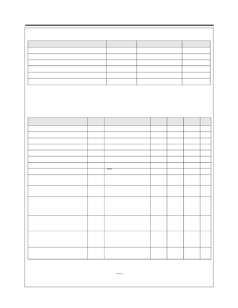 �
�
�N01L63W2A�
�Absolute� Maximum� Ratings� 1�
�Item�
�Voltage� on� any� pin� relative� to� V� SS�
�Voltage� on� V� CC� Supply� Relative� to� V� SS�
�Power� Dissipation�
�Storage� Temperature�
�Operating� Temperature�
�Soldering� Temperature� and� Time�
�Symbol�
�V� IN,OUT�
�V� CC�
�P� D�
�T� STG�
�T� A�
�T� SOLDER�
�Rating�
�–0.3� to� V� CC� +0.3�
�–0.3� to� 4.5�
�500�
�–40� to� 125�
�-40� to� +85�
�260� o� C,� 10sec�
�Unit�
�V�
�V�
�mW�
�o� C�
�o� C�
�o� C�
�1.� Stresses� greater� than� those� listed� above� may� cause� permanent� damage� to� the� device.� This� is� a� stress� rating� only� and� functional�
�operation� of� the� device� at� these� or� any� other� conditions� above� those� indicated� in� the� operating� section� of� this� specification� is� not�
�implied.� Exposure� to� absolute� maximum� rating� conditions� for� extended� periods� may� affect� reliability.�
�Operating� Characteristics� (Over� Specified� Temperature� Range)�
�Item�
�Supply� Voltage�
�Data� Retention� Voltage�
�Input� High� Voltage�
�Input� Low� Voltage�
�Symbol�
�V� CC�
�V� DR�
�V� IH�
�V� IL�
�Test� Conditions�
�3�
�Chip� Disabled�
�Min.�
�2.3�
�1.8�
�1.8�
�–0.3�
�Typ� 1�
�3.0�
�Max�
�3.6�
�V� CC� +0.3�
�0.6�
�Unit�
�V�
�V�
�V�
�V�
�Output� High� Voltage�
�Output� Low� Voltage�
�Input� Leakage� Current�
�Output� Leakage� Current�
�V� OH�
�V� OL�
�I� LI�
�I� LO�
�I� OH� =� 0.2mA�
�I� OL� =� -0.2mA�
�V� IN� =� 0� to� V� CC�
�OE� =� V� IH� or� Chip� Disabled�
�V� CC� –0.2�
�0.2�
�0.5�
�0.5�
�V�
�V�
�μ� A�
�μ� A�
�Read/Write� Operating� Supply� Current�
�@� 1� μ� s� Cycle� Time� 2�
�Read/Write� Operating� Supply� Current�
�@� 70� ns� Cycle� Time� 2�
�I� CC1�
�I� CC2�
�V� CC� =3.6� V,� V� IN� =V� IH� or� V� IL�
�Chip� Enabled,� I� OUT� =� 0�
�V� CC� =3.6� V,� V� IN� =V� IH� or� V� IL�
�Chip� Enabled,� I� OUT� =� 0�
�2.0�
�9.5�
�3.0�
�14.0�
�mA�
�mA�
�Page� Mode� Operating� Supply� Current�
�@� 70ns� Cycle� Time� 2� (Refer� to� Power�
�Savings� with� Page� Mode� Operation�
�I� CC3�
�V� CC� =3.6� V,� V� IN� =V� IH� or� V� IL�
�Chip� Enabled,� I� OUT� =� 0�
�4�
�mA�
�diagram)�
�Read/Write� Quiescent� Operating� Sup-�
�ply� Current� 3�
�I� CC4�
�V� CC� =3.6� V,� V� IN� =V� IH� or� V� IL�
�Chip� Enabled,� I� OUT� =� 0,�
�f=0�
�3.0�
�mA�
�V� IN� =� V� CC� or� 0V�
�Maximum� Standby� Current� 3�
�Maximum� Data� Retention� Current� 3�
�I� SB1�
�I� DR�
�Chip� Disabled�
�t� A� =� 85� o� C,� V� CC� =� 3.6� V�
�Vcc� =� 1.8V,� V� IN� =� V� CC� or� 0�
�Chip� Disabled,� t� A� =� 85� o� C�
�2.0�
�20�
�10�
�μ� A�
�μ� A�
�1.� Typical� values� are� measured� at� Vcc=Vcc� Typ.,� T� A� =25°C� and� not� 100%� tested.�
�2.� This� parameter� is� specified� with� the� outputs� disabled� to� avoid� external� loading� effects.� The� user� must� add� current� required� to� drive�
�output� capacitance� expected� in� the� actual� system.�
�3.� This� device� assumes� a� standby� mode� if� the� chip� is� disabled� (CE1� high� or� CE2� low).� In� order� to� achieve� low� standby� current� all�
�inputs� must� be� within� 0.2� volts� of� either� VCC� or� VSS�
�Rev.� 9� |� Page� 3� of� 10� |� www.onsemi.com�
�相关PDF资料 |
PDF描述 |
|---|---|
| N01L63W3AB25I | IC SRAM 1MBIT 3V LP 48-BGA |
| N01L83W2AN5I | IC SRAM 1MB ASYNC CMOS 3STSOP-I |
| N02L6181AB27I | IC SRAM 2MBIT 1.8V LP 48-BGA |
| N02L63W2AB25I | IC SRAM 2MBIT 3V LP 48-BGA |
| N02L63W3AT25IT | IC SRAM 2MBIT 3V LP 44-TSOP |
相关代理商/技术参数 |
参数描述 |
|---|---|
| N01L63W2AB25IT | 制造商:ONSEMI 制造商全称:ON Semiconductor 功能描述:1Mb Ultra-Low Power Asynchronous CMOS SRAM 64K × 16 bit |
| N01L63W2AB5I | 制造商:ONSEMI 制造商全称:ON Semiconductor 功能描述:1Mb Ultra-Low Power Asynchronous CMOS SRAM 64K × 16 bit |
| N01L63W2AB5IT | 制造商:ONSEMI 制造商全称:ON Semiconductor 功能描述:1Mb Ultra-Low Power Asynchronous CMOS SRAM 64K × 16 bit |
| N01L63W2AT25I | 功能描述:静态随机存取存储器 1MB 3V LOW PWR 静态随机存取存储器 RoHS:否 制造商:Cypress Semiconductor 存储容量:16 Mbit 组织:1 M x 16 访问时间:55 ns 电源电压-最大:3.6 V 电源电压-最小:2.2 V 最大工作电流:22 uA 最大工作温度:+ 85 C 最小工作温度:- 40 C 安装风格:SMD/SMT 封装 / 箱体:TSOP-48 封装:Tray |
| N01L63W2AT25IT | 制造商:ONSEMI 制造商全称:ON Semiconductor 功能描述:1Mb Ultra-Low Power Asynchronous CMOS SRAM 64K × 16 bit |
发布紧急采购,3分钟左右您将得到回复。