- 您现在的位置:买卖IC网 > PDF目录224594 > N74F109D-T (NXP SEMICONDUCTORS) Positive J-Knot positive edge-triggered flip-flops - Description: Dual J-/K Flip-Flop with Set and Reset; Positive-Edge Trigger ; F<sub>max</sub>: 125 MHz; Logic switching levels: TTL ; Number of pins: 14 ; Output drive capability: -1/+20 mA ; Propagation delay: 6.2 ns; Voltage: 4.5-5.5 V PDF资料下载
参数资料
| 型号: | N74F109D-T |
| 厂商: | NXP SEMICONDUCTORS |
| 元件分类: | 锁存器 |
| 英文描述: | Positive J-Knot positive edge-triggered flip-flops - Description: Dual J-/K Flip-Flop with Set and Reset; Positive-Edge Trigger ; F<sub>max</sub>: 125 MHz; Logic switching levels: TTL ; Number of pins: 14 ; Output drive capability: -1/+20 mA ; Propagation delay: 6.2 ns; Voltage: 4.5-5.5 V |
| 中文描述: | F/FAST SERIES, DUAL POSITIVE EDGE TRIGGERED J-KBAR FLIP-FLOP, COMPLEMENTARY OUTPUT, PDSO16 |
| 封装: | 3.9 MM, PLASTIC, SOT109-1, SO-16 |
| 文件页数: | 3/10页 |
| 文件大小: | 95K |
| 代理商: | N74F109D-T |
Philips Semiconductors
Product specification
74F109
Postive J-K positive edge-triggered flip-flops
2
October 23, 1990
853–0337 00783
FEATURE
Industrial temperature range available (–40°C to +85°C)
DESCRIPTION
The 74F109 is a dual positive edge-triggered JK-type flip-flop
featuring individual J, K, clock, set, and reset inputs; also true and
complementary outputs. Set (SD) and reset (RD) are asynchronous
active low inputs and operate independently of the clock (CP) input.
The J and K are edge-triggered inputs which control the state
changes of the flip-flops as described in the function table. Clock
triggering occurs at a voltage level and is not directly related to the
transition time of the positive-going pulse. The J and K inputs must
be stable just one setup time prior to the low-to-high transition of the
clock for predictable operation. The JK design allows operation as a
D flip-flop by tying J and K inputs together. Although the clock input
is level sensitive, the positive transition of the clock pulse between
the 0.8V and 2.0V levels should be equal to or less than the clock to
output delay time for reliable operation.
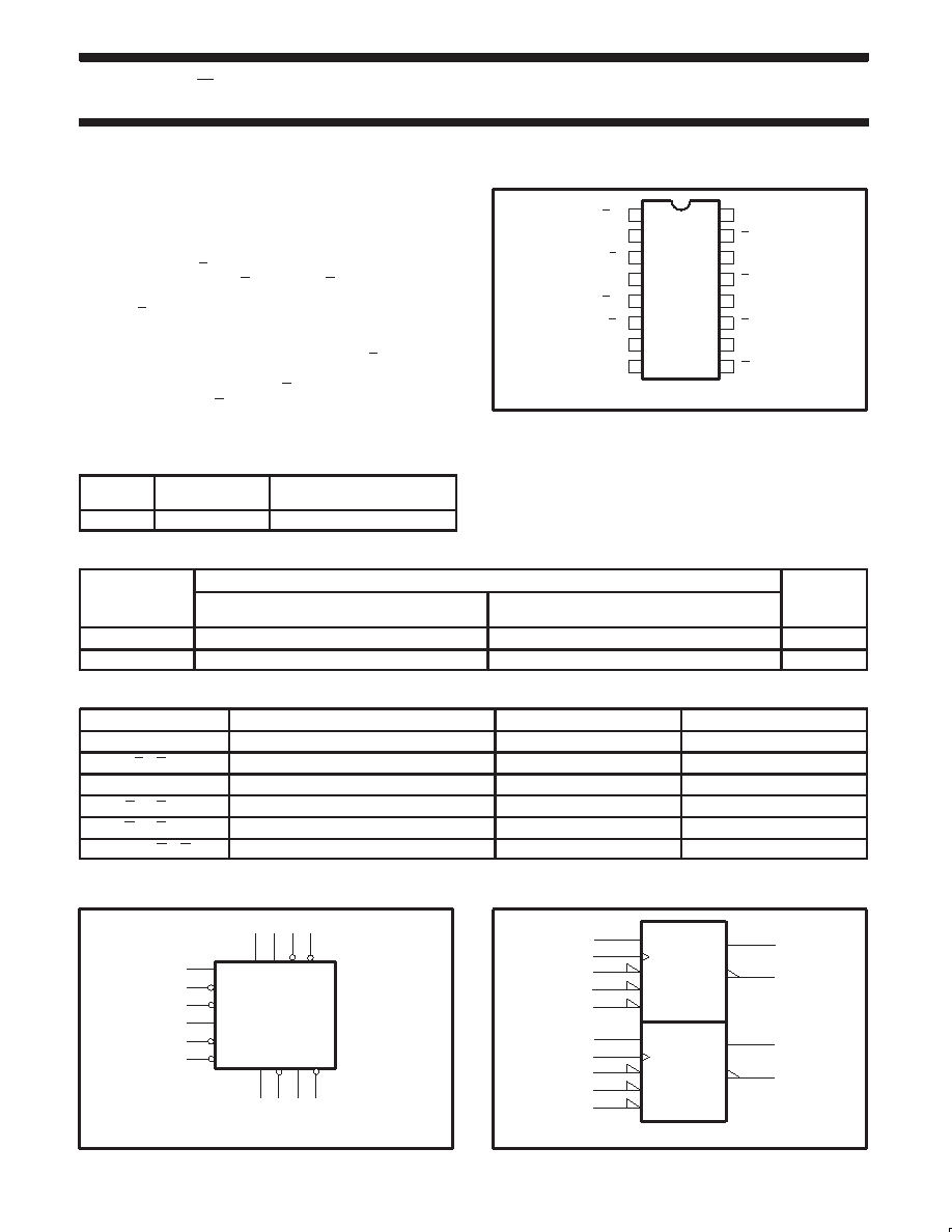
PIN CONFIGURATION
16
15
14
13
12
11
10
7
6
5
4
3
2
1
Q0
VCC
CP1
SD1
Q1
K1
RD1
J1
RD0
J0
Q0
K0
CP0
SD0
9
8
GND
Q1
SF00135
TYPE
TYPICAL fmax
TYPICAL SUPPLY CURRENT
(TOTAL)
74F109
125MHz
12.3mA
ORDERING INFORMATION
ORDER CODE
DESCRIPTION
COMMERCIAL RANGE
VCC = 5V ±10%, Tamb = 0°C to +70°C
INDUSTRIAL RANGE
VCC = 5V ±10%, Tamb = –40°C to +85°C
PKG DWG #
16-pin plastic DIP
N74F109N
I74F109N
SOT38-4
16-pin plastic SO
N74F109D
I74F109D
SOT109-1
INPUT AND OUTPUT LOADING AND FAN OUT TABLE
PINS
DESCRIPTION
74F (U.L.) HIGH/LOW
LOAD VALUE HIGH/LOW
J0, J1
J inputs
1.0/1.0
20
A/0.6mA
K0, K1
K inputs
1.0/1.0
20
A/0.6mA
CP0, CP1
Clock inputs (active rising edge)
1.0/1.0
20
A/0.6mA
SD0, SD1
Set inputs (active Low)
1.0/3.0
20
A/1.8mA
RD0, RD1
Reset inputs (active Low)
1.0/3.0
20
A/1.8mA
Q0, Q1, Q0, Q1
Data outputs
50/33
1.0mA/20mA
NOTE: One (1.0) FAST unit load is defined as: 20
A in the High state and 0.6mA in the Low state.
LOGIC SYMBOL
J1
J0
Q0 Q0 Q1 Q1
VCC = Pin 16
GND = Pin 8
K1
K0
2 14
3 13
6
7
10
9
CP0
SD0
RD0
CP1
SD1
RD1
4
5
1
12
11
15
SF00136
IEC/IEEE SYMBOL
SF00137
7
2
4
3
1
5
14
12
13
15
11
6
10
9
1J
C1
1K
R
S
2J
C2
2K
R
S
相关PDF资料 |
PDF描述 |
|---|---|
| N74F1244D-T | Octal buffer (3-State) - Description: Buffer/Light Load F244 (3-State) ; Logic switching levels: TTL ; Number of pins: 20 ; Output drive capability: -15/+64 mA ; Propagation delay: 5 ns; Voltage: 4.5-5.5 V |
| N74F125D-T | Quad buffers (3-State) - Description: Quad Buffer/Line Driver with Active LOW Output Enable (3-State) ; Logic switching levels: TTL ; Number of pins: 14 ; Output drive capability: -15/+64 mA ; Propagation delay: 5 ns; Voltage: 4.5-5.5 V |
| N74F126D-T | Quad buffers (3-State) - Description: Quad Buffer/Line Driver with Active HIGH Output Enable (3-State) ; Logic switching levels: TTL ; Number of pins: 14 ; Output drive capability: -15/+64 mA ; Propagation delay: 5 ns; Voltage: 4.5-5.5 V |
| N74F138D-T | 1-of-8 decoder/demultiplexer - Description: 3-to-8 Line Decoder/Demultiplexer; Inverting ; Logic switching levels: TTL ; Number of pins: 16 ; Output drive capability: -1/+20 mA ; Propagation delay: 6.1 ns; Voltage: 4.5-5.5 V |
| N74F139D-T | Dual 1-of-4 decoder/demultiplexer - Description: Dual 2-to-4 Line Decoder/Demultiplexer ; Logic switching levels: TTL ; Number of pins: 16 ; Output drive capability: -1/+20 mA ; Propagation delay: 5.3 ns; Voltage: 4.5-5.5 V |
相关代理商/技术参数 |
参数描述 |
|---|---|
| N74F109N | 功能描述:触发器 DUAL J-K POS EDGE RoHS:否 制造商:Texas Instruments 电路数量:2 逻辑系列:SN74 逻辑类型:D-Type Flip-Flop 极性:Inverting, Non-Inverting 输入类型:CMOS 输出类型: 传播延迟时间:4.4 ns 高电平输出电流:- 16 mA 低电平输出电流:16 mA 电源电压-最大:5.5 V 最大工作温度:+ 85 C 安装风格:SMD/SMT 封装 / 箱体:X2SON-8 封装:Reel |
| N74F109N,602 | 功能描述:触发器 DUAL J-K POS EDGE RoHS:否 制造商:Texas Instruments 电路数量:2 逻辑系列:SN74 逻辑类型:D-Type Flip-Flop 极性:Inverting, Non-Inverting 输入类型:CMOS 输出类型: 传播延迟时间:4.4 ns 高电平输出电流:- 16 mA 低电平输出电流:16 mA 电源电压-最大:5.5 V 最大工作温度:+ 85 C 安装风格:SMD/SMT 封装 / 箱体:X2SON-8 封装:Reel |
| N74F10D | 功能描述:逻辑门 TRIPLE 3-INPUT NAND GATE RoHS:否 制造商:Texas Instruments 产品:OR 逻辑系列:LVC 栅极数量:2 线路数量(输入/输出):2 / 1 高电平输出电流:- 16 mA 低电平输出电流:16 mA 传播延迟时间:3.8 ns 电源电压-最大:5.5 V 电源电压-最小:1.65 V 最大工作温度:+ 125 C 安装风格:SMD/SMT 封装 / 箱体:DCU-8 封装:Reel |
| N74F10D,602 | 功能描述:逻辑门 TRIPLE 3-INPUT NAND RoHS:否 制造商:Texas Instruments 产品:OR 逻辑系列:LVC 栅极数量:2 线路数量(输入/输出):2 / 1 高电平输出电流:- 16 mA 低电平输出电流:16 mA 传播延迟时间:3.8 ns 电源电压-最大:5.5 V 电源电压-最小:1.65 V 最大工作温度:+ 125 C 安装风格:SMD/SMT 封装 / 箱体:DCU-8 封装:Reel |
| N74F10D,623 | 功能描述:逻辑门 TRIPLE 3-INPUT NAND RoHS:否 制造商:Texas Instruments 产品:OR 逻辑系列:LVC 栅极数量:2 线路数量(输入/输出):2 / 1 高电平输出电流:- 16 mA 低电平输出电流:16 mA 传播延迟时间:3.8 ns 电源电压-最大:5.5 V 电源电压-最小:1.65 V 最大工作温度:+ 125 C 安装风格:SMD/SMT 封装 / 箱体:DCU-8 封装:Reel |
发布紧急采购,3分钟左右您将得到回复。