- 您现在的位置:买卖IC网 > PDF目录189001 > NAND512R4A0BZA6 (NUMONYX) 32M X 16 FLASH 1.8V PROM, 35 ns, PBGA63 PDF资料下载
参数资料
| 型号: | NAND512R4A0BZA6 |
| 厂商: | NUMONYX |
| 元件分类: | PROM |
| 英文描述: | 32M X 16 FLASH 1.8V PROM, 35 ns, PBGA63 |
| 封装: | 9 X 11 MM, 1 MM HEIGHT, 0.80 MM PITCH, VFBGA-63 |
| 文件页数: | 13/57页 |
| 文件大小: | 916K |
| 代理商: | NAND512R4A0BZA6 |
第1页第2页第3页第4页第5页第6页第7页第8页第9页第10页第11页第12页当前第13页第14页第15页第16页第17页第18页第19页第20页第21页第22页第23页第24页第25页第26页第27页第28页第29页第30页第31页第32页第33页第34页第35页第36页第37页第38页第39页第40页第41页第42页第43页第44页第45页第46页第47页第48页第49页第50页第51页第52页第53页第54页第55页第56页第57页
NAND128-A, NAND256-A, NAND512-A, NAND01G-A
20/57
DEVICE OPERATIONS
Pointer Operations
As the NAND Flash memories contain two differ-
ent areas for x16 devices and three different areas
for x8 devices (see Figure 11.) the read command
codes (00h, 01h, 50h) are used to act as pointers
to the different areas of the memory array (they se-
lect the most significant column address).
The Read A and Read B commands act as point-
ers to the main memory area. Their use depends
on the bus width of the device.
■
In x16 devices the Read A command (00h)
sets the pointer to Area A (the whole of the
main area) that is Words 0 to 255.
■
In x8 devices the Read A command (00h) sets
the pointer to Area A (the first half of the main
area) that is Bytes 0 to 255, and the Read B
command (01h) sets the pointer to Area B (the
second half of the main area) that is Bytes 256
to 511.
In both the x8 and x16 devices the Read C com-
mand (50h), acts as a pointer to Area C (the spare
memory area) that is Bytes 512 to 527 or Words
256 to 263.
Once the Read A and Read C commands have
been issued the pointer remains in the respective
areas until another pointer code is issued. Howev-
er, the Read B command is effective for only one
operation, once an operation has been executed
in Area B the pointer returns automatically to Area
A.
The pointer operations can also be used before a
program operation, that is the appropriate code
(00h, 01h or 50h) can be issued before the pro-
gram command 80h is issued (see Figure 12.).
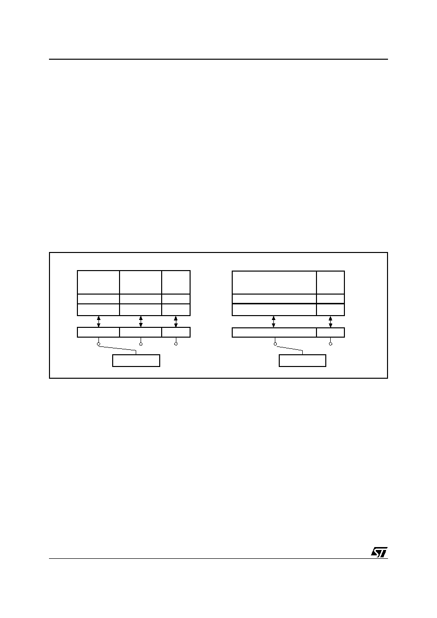
Figure 11. Pointer Operations
AI07592
Area A
(00h)
A
Area B
(01h)
Area C
(50h)
Bytes 0- 255
Bytes 256-511
Bytes 512
-527
C
B
Pointer
(00h,01h,50h)
Page Buffer
Area A
(00h)
A
Area C
(50h)
Words 0- 255
Words 256
-263
C
Pointer
(00h,50h)
Page Buffer
x8 Devices
x16 Devices
相关PDF资料 |
PDF描述 |
|---|---|
| NAND512R4A0BZB6 | 32M X 16 FLASH 1.8V PROM, 35 ns, PBGA55 |
| NAND512R4A0CZA6T | 32M X 16 FLASH 1.8V PROM, 35 ns, PBGA63 |
| NAND512R4A2CZB6F | 32M X 16 FLASH 1.8V PROM, 35 ns, PBGA55 |
| NAND512W3A0AN1 | 64M X 8 FLASH 3V PROM, 35 ns, PDSO48 |
| NAND512W3A0CZB6 | 64M X 8 FLASH 3V PROM, 35 ns, PBGA55 |
相关代理商/技术参数 |
参数描述 |
|---|---|
| NAND512R4A2CWFD | 制造商:Micron Technology Inc 功能描述:NAND - Gel-pak, waffle pack, wafer, diced wafer on film |
| NAND512R4A2CZA6 | 制造商:Micron Technology Inc 功能描述:512MB. 3V X8 NO OPTION TSOP48TSOP-1 48 12X20 AL 42 - Trays |
| NAND512R4A2DDI6 | 制造商:Micron Technology Inc 功能描述:NAND - Gel-pak, waffle pack, wafer, diced wafer on film |
| NAND512W3A0AN6 | 功能描述:闪存 NAND & S.MEDIA FLASH RoHS:否 制造商:ON Semiconductor 数据总线宽度:1 bit 存储类型:Flash 存储容量:2 MB 结构:256 K x 8 定时类型: 接口类型:SPI 访问时间: 电源电压-最大:3.6 V 电源电压-最小:2.3 V 最大工作电流:15 mA 工作温度:- 40 C to + 85 C 安装风格:SMD/SMT 封装 / 箱体: 封装:Reel |
| NAND512W3A0AN6E | 功能描述:闪存 2.7-3.6V 512M(64Mx8) RoHS:否 制造商:ON Semiconductor 数据总线宽度:1 bit 存储类型:Flash 存储容量:2 MB 结构:256 K x 8 定时类型: 接口类型:SPI 访问时间: 电源电压-最大:3.6 V 电源电压-最小:2.3 V 最大工作电流:15 mA 工作温度:- 40 C to + 85 C 安装风格:SMD/SMT 封装 / 箱体: 封装:Reel |
发布紧急采购,3分钟左右您将得到回复。