参数资料
| 型号: | NB3N201SDR2G |
| 厂商: | ON Semiconductor |
| 文件页数: | 16/19页 |
| 文件大小: | 0K |
| 描述: | IC CLK DVR RECEIVER M-LVDS 8SOIC |
| 标准包装: | 2,500 |
| 类型: | 缓冲器/驱动器 |
| 电路数: | 1 |
| 比率 - 输入:输出: | 1:1 |
| 差分 - 输入:输出: | 是/是 |
| 输入: | LVCMOS,LVDS |
| 输出: | LVCMOS,LVDS |
| 频率 - 最大: | 200MHz |
| 电源电压: | 3 V ~ 3.6 V |
| 工作温度: | -40°C ~ 85°C |
| 安装类型: | 表面贴装 |
| 封装/外壳: | 8-SOIC(0.154",3.90mm 宽) |
| 供应商设备封装: | 8-SOIC |
| 包装: | 带卷 (TR) |
NB3N201S, NB3N206S
http://onsemi.com
6
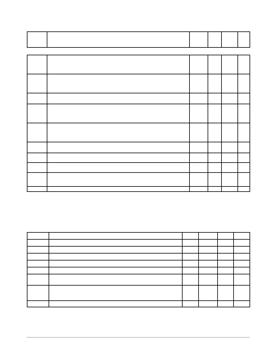
Table 5. DC CHARACTERISTICS VCC = 3.3 ±10% V( 3.0 to 3.6 V), GND = 0 V, TA = 40°C to +85°C (See Notes 4, 5)
Symbol
Characteristic
Min
Typ
(Note
Max
Unit
BUS INPUT AND OUTPUT
IA
Input Current Receiver or Transceiver with Driver Disabled
VA = 3.8 V, VB = 1.2 V
VA = 0.0 V or 2.4 V, VB = 1.2 V
VA = 1.4 V, VB = 1.2 V
0
20
32
20
0
uA
IB
Input Current Receiver or Transceiver with Driver Disabled
VB = 3.8 V, VA = 1.2 V
VB = 0.0 V or 2.4 V, VA = 1.2 V
VB = 1.4 V, VA = 1.2 V
0
20
32
20
0
uA
IAB
Differential Input Current Receiver or Transceiver with driver disabled (IAIB)
VA = VB , 1.4 ≤ VA ≤ 3.8 V
4
uA
IA(OFF)
Input Current Receiver or Transceiver Power Off 0V ≤ VCC ≤ 1.5 and:
VA = 3.8 V, VB = 1.2 V
VA = 0.0 V or 2.4 V, VB = 1.2 V
VA = 1.4 V, VB = 1.2 V
0
20
32
20
0
uA
IB(OFF)
Input Current Receiver or Transceiver Power Off 0V ≤ VCC ≤ 1.5 and:
VB = 3.8 V, VA = 1.2 V
VB = 0.0 V or 2.4 V, VA = 1.2 V
VB = 1.4 V, VA = 1.2 V
0
20
32
20
0
uA
IAB(OFF)
Receiver Input or Transceiver Input/Output Power Off Differential Input Current; (IAIB)
VA = VB , 0 ≤ VCC ≤ 1.5 V, 1.4 ≤ VA ≤ 3.8 V
4
uA
CA
Transceiver Input Capacitance with Driver Disabled VA = 0.4 sin(30E6πt) + 0.5 V using
HP4194A impedance analyzer (or equivalent); VB = 1.2 V
5
pF
CB
Transceiver Input Capacitance with Driver Disabled VB = 0.4 sin(30E6πt) + 0.5 V using
HP4194A impedance analyzer (or equivalent); VA = 1.2 V
5
pF
CAB
Transceiver Differential Input Capacitance with Driver Disabled VA = 0.4 sin(30E6pt) +
0.5 V using HP4194A impedance analyzer (or equivalent);
VB = 1.2 V
3.0
pF
CA/B
Transceiver Input Capacitance Balance with Driver Disabled, (CA/CB)
99
101
%
NOTE: Device will meet the specifications after thermal equilibrium has been established when mounted in a test socket or printed circuit
board with maintained transverse airflow greater than 500 lfpm. Electrical parameters are guaranteed only over the declared
operating temperature range. Functional operation of the device exceeding these conditions is not implied. Device specification limit
values are applied individually under normal operating conditions and not valid simultaneously.
4. See Figure 3. DC Measurements reference.
5. Typ value at 25°C and 3.3 VCC supply voltage.
Table 6. DRIVER AC CHARACTERISTICS VCC = 3.3 ±10% V( 3.0 to 3.6 V), GND = 0 V, TA = 40°C to +85°C (Note 6)
Symbol
Characteristic
Min
Typ
Max
Unit
tPLH / tPHL
Propagation Delay (See Figure 7)
1.0
1.5
2.4
ns
tPHZ / tPLZ
Disable Time HIGH or LOW state to High Impedance (See Figure 8)
7
ns
tPZH / tPZL
Enable Time High Impedance to HIGH or LOW state (See Figure 8)
7
ns
tSK(P)
0
100
ps
tSK(PP)
Device to Device Skew similar path and conditions (See Figure 7)
1
ns
tJIT(PER)
Period Jitter RMS, 100 MHz (Source tr/tf 0.5 ns, 10 and 90 % points, 30k
samples. Source jitter deembedded from Output values ) (See Figure 10)
2
3
ps
tJIT(PP)
Peaktopeak Jitter, 200 Mbps 2151 PRBS (Source tr/tf 0.5 ns, 10 and 90%
points, 100k samples. Source jitter deembedded from Output values) (See
Figure 10)
30
130
ps
tr / tf
Differential Output rise and fall times (See Figure 7)
1
1.6
ns
NOTE: Device will meet the specifications after thermal equilibrium has been established when mounted in a test socket or printed circuit
board with maintained transverse airflow greater than 500 lfpm. Electrical parameters are guaranteed only over the declared
operating temperature range. Functional operation of the device exceeding these conditions is not implied. Device specification limit
values are applied individually under normal operating conditions and not valid simultaneously.
6. Typ value at 25°C and 3.3 VCC supply voltage.
相关PDF资料 |
PDF描述 |
|---|---|
| NB3N200SDR2G | IC CLK DVR RECEIVER M-LVDS 8SOIC |
| V300A36H400BL3 | CONVERTER MOD DC/DC 36V 400W |
| AD5663RBCPZ-3REEL7 | IC DAC NANO 16BIT 1.25V 10-LFCSP |
| V300A36H400BL2 | CONVERTER MOD DC/DC 36V 400W |
| AD7305BRZ-REEL | IC DAC 8BIT QUAD R-R 20SOIC |
相关代理商/技术参数 |
参数描述 |
|---|---|
| NB3N206SDG | 功能描述:时钟缓冲器 M-LVDS DRIVER RECEIVER RoHS:否 制造商:Texas Instruments 输出端数量:5 最大输入频率:40 MHz 传播延迟(最大值): 电源电压-最大:3.45 V 电源电压-最小:2.375 V 最大功率耗散: 最大工作温度:+ 85 C 最小工作温度:- 40 C 封装 / 箱体:LLP-24 封装:Reel |
| NB3N206SDR2G | 功能描述:时钟缓冲器 M-LVDS DRIVER RECEIVER RoHS:否 制造商:Texas Instruments 输出端数量:5 最大输入频率:40 MHz 传播延迟(最大值): 电源电压-最大:3.45 V 电源电压-最小:2.375 V 最大功率耗散: 最大工作温度:+ 85 C 最小工作温度:- 40 C 封装 / 箱体:LLP-24 封装:Reel |
| NB3N2302DG | 功能描述:时钟缓冲器 FREQ MULTIPLIER AND ZDB RoHS:否 制造商:Texas Instruments 输出端数量:5 最大输入频率:40 MHz 传播延迟(最大值): 电源电压-最大:3.45 V 电源电压-最小:2.375 V 最大功率耗散: 最大工作温度:+ 85 C 最小工作温度:- 40 C 封装 / 箱体:LLP-24 封装:Reel |
| NB3N2302DR2G | 功能描述:时钟缓冲器 FREQ MULTIPLIER AND ZDB RoHS:否 制造商:Texas Instruments 输出端数量:5 最大输入频率:40 MHz 传播延迟(最大值): 电源电压-最大:3.45 V 电源电压-最小:2.375 V 最大功率耗散: 最大工作温度:+ 85 C 最小工作温度:- 40 C 封装 / 箱体:LLP-24 封装:Reel |
| NB3N2304ND | 制造商:ONSEMI 制造商全称:ON Semiconductor 功能描述:3.3V 1:4 Clock Fanout Buffer |
发布紧急采购,3分钟左右您将得到回复。