参数资料
| 型号: | NB3N49152MNTXG |
| 厂商: | ON Semiconductor |
| 文件页数: | 3/6页 |
| 文件大小: | 0K |
| 描述: | IC CLK GEN VCXO LVPECL 20QFN |
| 标准包装: | 3,000 |
| 系列: | PureEdge™ |
| 类型: | * |
| PLL: | 无 |
| 输入: | 晶体 |
| 输出: | LVPECL |
| 电路数: | 1 |
| 比率 - 输入:输出: | 1:1 |
| 差分 - 输入:输出: | 无/是 |
| 频率 - 最大: | 491.52MHz |
| 除法器/乘法器: | 无/是 |
| 电源电压: | 2.97 V ~ 3.63 V |
| 工作温度: | -40°C ~ 85°C |
| 安装类型: | 表面贴装 |
| 封装/外壳: | 20-VFQFN 裸露焊盘 |
| 供应商设备封装: | 20-QFN(4x4) |
| 包装: | 带卷 (TR) |
NB3Nxxxxx VCXO Series
http://onsemi.com
3
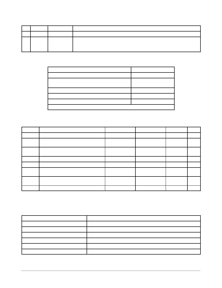
Table 2. PIN DESCRIPTION
Pin
Description
I/O
Name
20
nc
No connect
EP
The Exposed Pad (EP) on the QFN20 package bottom is thermally connected to the die for
improved heat transfer out of package. The exposed pad must be attached to a heatsinking
conduit. The pad is electrically connected to the die, and must be electrically and thermally
connected to GND on the PC board.
1. All VDD and GND pins must be externally connected to a power supply for proper operation.
Table 3. ATTRIBUTES
Characteristics
Value
Internal Default State Resistor (OE)
170 kW
ESD Protection Human Body Model
Machine Model
2 kV
200 V
Moisture Sensitivity, Indefinite Time Out of Drypack (Note 2)
Level 1
Flammability Rating Oxygen Index: 28 to 34
UL 94 V0 @ 0.125 in
Transistor Count
3510 Devices
Meets or Exceeds JEDEC Standard EIA/JESD78 IC Latchup Test
2. For additional information, see Application Note AND8003/D.
Table 4. MAXIMUM RATINGS
Symbol
Parameter
Condition 1
Rating
Unit
VDD
Positive Power Supply
GND = 0 V
4.6
V
VIN
Control Input (VC and OE)
VIN ≤ VDD + 200 mV
VIN ≥ GND 200 mV
V
IOUT
LVPECL Output Current
Continuous
Surge
25
50
mA
TA
Operating Temperature Range
40 to +85
°C
Tstg
Storage Temperature Range
55 to +120
°C
qJA
Thermal Resistance (JunctiontoAmbient)
0 lfpm
500 lfpm
QFN20
47
33
°C/W
qJC
Thermal Resistance (JunctiontoCase)
(Note 3)
Standard Board
QFN20
18
°C/W
Tsol
Wave Solder PbFree
265
°C
Stresses exceeding Maximum Ratings may damage the device. Maximum Ratings are stress ratings only. Functional operation above the
Recommended Operating Conditions is not implied. Extended exposure to stresses above the Recommended Operating Conditions may affect
device reliability.
3. JEDEC standard multilayer board 2S2P (2 signal, 2 power) with 8 filled thermal vias under exposed pad.
Table 5. RECOMMENDED CRYSTAL PARAMETERS
Crystal Type
Fundamental ATCut
Frequency
Various Device dependent; see AC Table
Load Capacitance
16 pF
Shunt Capacitance, C0
3.2 pF typical
Motional Capacitance (C1)
12 fF typical
Capacitance Ratio (C0/C1)
260 typical
ESR (Equivalent Series Resistance)
25 W max; 5 W typical
相关PDF资料 |
PDF描述 |
|---|---|
| VI-JV1-MZ-F1 | CONVERTER MOD DC/DC 12V 25W |
| VI-25D-MW-F4 | CONVERTER MOD DC/DC 85V 100W |
| VE-B1Y-MY-F1 | CONVERTER MOD DC/DC 3.3V 33W |
| VE-B1Y-MX-F4 | CONVERTER MOD DC/DC 3.3V 49.5W |
| MS27656T25B4PA | CONN RCPT 56POS WALL MNT W/PINS |
相关代理商/技术参数 |
参数描述 |
|---|---|
| NB3N501 | 制造商:ONSEMI 制造商全称:ON Semiconductor 功能描述:3.3V / 5.0V 13 MHz to 160 MHz PLL Clock Multiplier |
| NB3N501DG | 功能描述:时钟缓冲器 PLL CLOCK MULTIPLIER RoHS:否 制造商:Texas Instruments 输出端数量:5 最大输入频率:40 MHz 传播延迟(最大值): 电源电压-最大:3.45 V 电源电压-最小:2.375 V 最大功率耗散: 最大工作温度:+ 85 C 最小工作温度:- 40 C 封装 / 箱体:LLP-24 封装:Reel |
| NB3N501DR2G | 功能描述:时钟缓冲器 PLL CLOCK MULTIPLIER RoHS:否 制造商:Texas Instruments 输出端数量:5 最大输入频率:40 MHz 传播延迟(最大值): 电源电压-最大:3.45 V 电源电压-最小:2.375 V 最大功率耗散: 最大工作温度:+ 85 C 最小工作温度:- 40 C 封装 / 箱体:LLP-24 封装:Reel |
| NB3N502 | 制造商:ONSEMI 制造商全称:ON Semiconductor 功能描述:14 MHz to 190 MHz PLL Clock Multiplier |
| NB3N502DEVB | 功能描述:时钟和定时器开发工具 EVALUATION BRD RoHS:否 制造商:Texas Instruments 产品:Evaluation Modules 类型:Clock Conditioners 工具用于评估:LMK04100B 频率:122.8 MHz 工作电源电压:3.3 V |
发布紧急采购,3分钟左右您将得到回复。