参数资料
| 型号: | NB3N65027DTR2G |
| 厂商: | ON Semiconductor |
| 文件页数: | 1/7页 |
| 文件大小: | 0K |
| 描述: | IC CLK SYNTHESIZER 3PLL 20QSOP |
| 标准包装: | 1 |
| 类型: | * |
| PLL: | 是 |
| 输入: | LVCMOS,LVTTL,晶体 |
| 输出: | LVCMOS,LVTTL |
| 电路数: | 1 |
| 比率 - 输入:输出: | 1:7 |
| 差分 - 输入:输出: | 无/无 |
| 频率 - 最大: | 125MHz |
| 除法器/乘法器: | 是/是 |
| 电源电压: | 3 V ~ 3.6 V |
| 工作温度: | -40°C ~ 85°C |
| 安装类型: | 表面贴装 |
| 封装/外壳: | 20-SSOP(0.154",3.90mm 宽) |
| 供应商设备封装: | 20-QSOP |
| 包装: | 标准包装 |
| 其它名称: | NB3N65027DTR2GOSDKR |
Semiconductor Components Industries, LLC, 2011
June, 2011 Rev. 2
1
Publication Order Number:
NB3N65027/D
NB3N65027
3.3V Programmable 3-PLL Clock
Synthesizer with
6 LVTTL/LVCMOS Outputs w/OE
The NB3N65027 is a LVCMOS PLLsynthesized clock generator.
It accepts a 10 MHz to 27 MHz clock or fundamental mode crystal as
the reference source and drives three independent, low noise
phaselocked loops (PLLs).
Control lines ACSx, BCSx and CCS will select their appropriate
bank output frequencies. ACS1 and BCS1 are twolevel
LVTTL/LVCMOS inputs, High and Low. ACS0, BCS0 and CCS are
threelevel LVCMOS inputs, High, Mid and Low.
The NB3N65027 has three independent LVTTL/LVCMOS output
banks of two outputs each. Banks A and B offer a 1X and a 1/2X
output. Using a 25 MHz crystal, the selectable output frequencies
range from 16 2/3 MHz to 133 1/3 MHz. A 12.5 MHz crystal offers
from 8 1/3 MHz to 66 2/3 MHz. In addition, the NB3N65027 will
generate a buffered reference LVTTL/LVCMOS output, REFOUT,
output frequencies. The OE pin, when set LOW, will disable the output
drivers to high impedance.
The NB3N65027 operates from a single +3.3 V supply across the
operating temperature range from 40
°C to +85°C, and is offered in a
QSOP20 RoHS compliant package.
The NB3N65027 provides the optimum combination of low cost,
flexibility, and high performance for Network, PCI and SDRAM
applications.
Features
12.5 MHz or 25 MHz Fundamental Crystal or Clock
Input
Six Output Clocks with Selectable Frequencies
Buffered Crystal Reference Output
SDRAM Frequencies of 67, 83, 100, and 133 MHz
LVCMOS with 25 mA Output Drive Capability at TTL
Levels
Operating Range: VCC = 3.3 V ±10%
QSOP20 Package, 150 mil
40°C to +85°C Ambient Operating Temperature
These Devices are PbFree and are RoHS Compliant
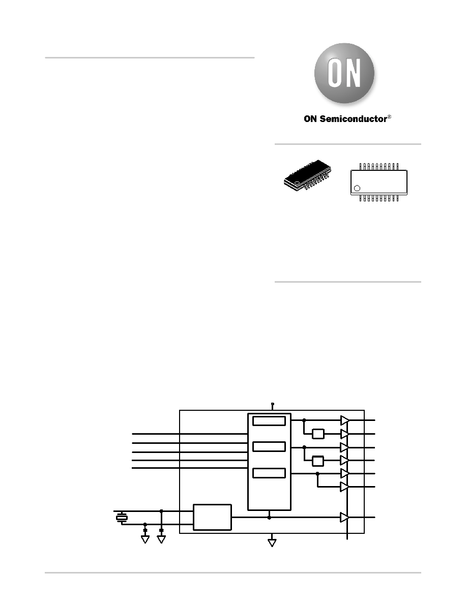
Figure 1. Simplified Logic Diagram
Buffer /
Oscillator
Clock
Synthesis
and Control
Circuitry
25 or 12.5 MHz
crystal or clock
ACS1
CLKA1
GND
X1/ICLK
X2
CLKA2
CLKB1
CLKB2
CLKC1
CLKC2
REFOUT
VDD
OE (all outputs)
ACS0
BCS1
BCS0
B2
CCS
PLLC
PLLB
PLLA
CLX2
CLX1
QSOP20
CASE 492AC
MARKING DIAGRAM
http://onsemi.com
3N65027 = Specific Device Code
A
= Assembly Location
WL
= Wafer Lot
Y
= Year
WW
= Work Week
G
= PbFree Package
See detailed ordering and shipping information in the package
dimensions section on page 6 of this data sheet.
ORDERING INFORMATION
3N65027
AWLYWWG
相关PDF资料 |
PDF描述 |
|---|---|
| MM74HCT138MTC | IC DECODER 3-TO-8 LINE 16-TSSOP |
| V28A48H200BL | CONVERTER MOD DC/DC 48V 200W |
| MS3450L28-2PX | CONN RCPT 14POS WALL MNT W/PINS |
| V28A48H200B3 | CONVERTER MOD DC/DC 48V 200W |
| MS3450L28-2PW | CONN RCPT 14POS WALL MNT W/PINS |
相关代理商/技术参数 |
参数描述 |
|---|---|
| NB3N853501EDTG | 功能描述:时钟驱动器及分配 2:1:4 LVPECL FAN-OUT BUFF RoHS:否 制造商:Micrel 乘法/除法因子:1:4 输出类型:Differential 最大输出频率:4.2 GHz 电源电压-最大: 电源电压-最小:5 V 最大工作温度:+ 85 C 封装 / 箱体:SOIC-8 封装:Reel |
| NB3N853501EDTR2G | 功能描述:时钟驱动器及分配 2:1:4 LVPECL FAN-OUT BUFF RoHS:否 制造商:Micrel 乘法/除法因子:1:4 输出类型:Differential 最大输出频率:4.2 GHz 电源电压-最大: 电源电压-最小:5 V 最大工作温度:+ 85 C 封装 / 箱体:SOIC-8 封装:Reel |
| NB3N853531EDTG | 功能描述:时钟缓冲器 FAN-OUT BUFF W/CRYSL INPT RoHS:否 制造商:Texas Instruments 输出端数量:5 最大输入频率:40 MHz 传播延迟(最大值): 电源电压-最大:3.45 V 电源电压-最小:2.375 V 最大功率耗散: 最大工作温度:+ 85 C 最小工作温度:- 40 C 封装 / 箱体:LLP-24 封装:Reel |
| NB3N853531EDTR2G | 功能描述:时钟缓冲器 FAN-OUT BUFF W/CRYSL INPT RoHS:否 制造商:Texas Instruments 输出端数量:5 最大输入频率:40 MHz 传播延迟(最大值): 电源电压-最大:3.45 V 电源电压-最小:2.375 V 最大功率耗散: 最大工作温度:+ 85 C 最小工作温度:- 40 C 封装 / 箱体:LLP-24 封装:Reel |
| NB3QKBA04 | 制造商:OMRON AUTOMATION AND SAFETY 功能描述:NB3 HMI PROTECTIVE SHEETS X5 |
发布紧急采购,3分钟左右您将得到回复。