参数资料
| 型号: | NB4L16MMN |
| 厂商: | ON Semiconductor |
| 文件页数: | 8/12页 |
| 文件大小: | 0K |
| 描述: | IC CLK BUFFER DVR TRANSLA 16-QFN |
| 产品变化通告: | Product Discontinuation 20/Aug/2008 |
| 标准包装: | 123 |
| 类型: | 缓冲器/驱动器,变换器 |
| 电路数: | 1 |
| 比率 - 输入:输出: | 2:1 |
| 差分 - 输入:输出: | 是/是 |
| 输入: | CML,HSTL,LVCMOS,LVDS,LVPECL,LVTTL |
| 输出: | CML |
| 频率 - 最大: | 3.5GHz |
| 电源电压: | 2.375 V ~ 3.8 V |
| 工作温度: | -40°C ~ 85°C |
| 安装类型: | 表面贴装 |
| 封装/外壳: | 16-VFQFN 裸露焊盘 |
| 供应商设备封装: | 16-QFN(3x3) |
| 包装: | 管件 |
NB4L16M
http://onsemi.com
5
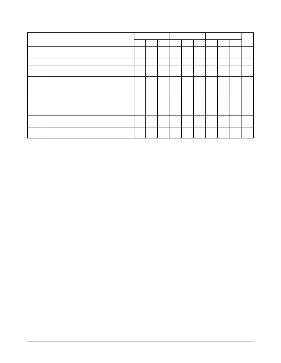
Symbol
Characteristic
40°C
25°C
85°C
Unit
Min
Typ
Max
Min
Typ
Max
Min
Typ
Max
VOUTPP Output Voltage Amplitude (@VINPPmin)fin ≤ 3.5 GHz
fin ≤ 4.5 GHz
280
150
400
300
280
150
400
300
280
150
400
300
mV
fDATA
Maximum Operating Data Rate
3.5
5.0
3.5
5.0
3.5
5.0
Gb/s
tPLH,
tPHL
Propagation Delay to Output Differential @ 0.5 GHz
(Figure 6)
175
215
265
175
220
265
175
225
265
ps
tSKEW
Duty Cycle Skew (Note 9)
DevicetoDevice Skew (Note 13)
2.0
6.0
10
90
2.0
6.0
10
90
2.0
6.0
10
90
ps
tJITTER
RMS Random Clock Jitter (Note 11)
fin ≤ 4.5 GHz
PeaktoPeak Data Dependent Jitter
(Note 12)
fDATA = 2.5 Gb/s
fDATA = 3.5 Gb/s
fDATA = 5.0 Gb/s
0.2
1.5
2.0
9.0
0.7
10
12
25
0.2
1.5
2.0
9.0
0.7
10
12
25
0.2
1.5
2.0
9.0
0.7
10
12
25
ps
VINPP
Input Voltage Swing/Sensitivity
(Differential Configuration) (Note 10)
75
VCC
VEE
75
VCC
VEE
75
VCC
VEE
mV
tr
tf
Output Rise/Fall Times @ 0.5 GHz
(Figure 5)
(20% 80%)
60
90
60
90
60
90
ps
NOTE: Device will meet the specifications after thermal equilibrium has been established when mounted in a test socket or printed circuit
board with maintained transverse airflow greater than 500 lfpm. Electrical parameters are guaranteed only over the declared
operating temperature range. Functional operation of the device exceeding these conditions is not implied. Device specification limit
values are applied individually under normal operating conditions and not valid simultaneously.
8. Measured by forcing VINPP(MIN) from a 50% duty cycle clock source. All loading with an external RL = 50 W to VCC. Input edge rates 40 ps
9. Duty cycle skew is measured between differential outputs using the deviations of the sum of Tpw and Tpw+ @ 0.5 GHz.
10.VINPP(MAX) cannot exceed VCC VEE. Input voltage swing is a singleended measurement operating in differential mode. See Figure 11.
11. Additive RMS jitter with 50% duty cycle input clock signal.
12.Additive peaktopeak data dependent jitter with NRZ input data signal, PRBS 2231 and K28.7 pattern. See Figures 7, 8, 9, 10, 11 and 12.
13.Devicetodevice skew is measured between outputs under identical transition @ 0.5 GHz.
相关PDF资料 |
PDF描述 |
|---|---|
| LTC1591-1CG#PBF | IC D/A CONV 14BIT PAR 28-SSOP |
| LTC1591-1CG | IC D/A CONV 14BIT PAR 28-SSOP |
| MC10LVEP11DR2 | IC CLOCK BUFFER 1:2 3GHZ 8-SOIC |
| LTC1657LCGN#PBF | IC DAC 16BIT R-R MICROPWR 28SSOP |
| NB7L14MMN | IC CLK/DTA BUF TRNSLA 1:4 16-QFN |
相关代理商/技术参数 |
参数描述 |
|---|---|
| NB4L16MMNEVB | 功能描述:其他开发工具 BBG NB4L16MMN EVAL BOARD RoHS:否 制造商:Parallax 产品:ELEV-8 Hex Upgrade Kits 类型:Robotics 工具用于评估:ELEV-8 Quadcopter 工作电源电压: |
| NB4L16MMNG | 功能描述:转换 - 电压电平 2.5V/3.3V 5Gb/s Driver/RCVR/Buffer RoHS:否 制造商:Micrel 类型:CML/LVDS/LVPECL to LVCMOS/LVTTL 传播延迟时间:1.9 ns 电源电流:14 mA 电源电压-最大:3.6 V 电源电压-最小:3 V 最大工作温度:+ 85 C 安装风格:SMD/SMT 封装 / 箱体:MLF-8 |
| NB4L16MMNR2 | 功能描述:转换 - 电压电平 2.5V/3.3V 5Gb/s RoHS:否 制造商:Micrel 类型:CML/LVDS/LVPECL to LVCMOS/LVTTL 传播延迟时间:1.9 ns 电源电流:14 mA 电源电压-最大:3.6 V 电源电压-最小:3 V 最大工作温度:+ 85 C 安装风格:SMD/SMT 封装 / 箱体:MLF-8 |
| NB4L16MMNR2G | 功能描述:转换 - 电压电平 2.5V/3.3V 5Gb/s Driver/RCVR/Buffer RoHS:否 制造商:Micrel 类型:CML/LVDS/LVPECL to LVCMOS/LVTTL 传播延迟时间:1.9 ns 电源电流:14 mA 电源电压-最大:3.6 V 电源电压-最小:3 V 最大工作温度:+ 85 C 安装风格:SMD/SMT 封装 / 箱体:MLF-8 |
| NB4L339 | 制造商:ONSEMI 制造商全称:ON Semiconductor 功能描述:3.3V 1:4 Clock Fanout Buffer |
发布紧急采购,3分钟左右您将得到回复。