参数资料
| 型号: | NB7L14MMN |
| 厂商: | ON Semiconductor |
| 文件页数: | 1/11页 |
| 文件大小: | 0K |
| 描述: | IC CLK/DTA BUF TRNSLA 1:4 16-QFN |
| 产品变化通告: | LTB Notification 06/Feb/2008 |
| 标准包装: | 123 |
| 类型: | 扇出缓冲器(分配),变换器,数据 |
| 电路数: | 1 |
| 比率 - 输入:输出: | 1:4 |
| 差分 - 输入:输出: | 是/是 |
| 输入: | CML,LVCMOS,LVDS,LVPECL,LVTTL |
| 输出: | CML |
| 频率 - 最大: | 8GHz |
| 电源电压: | 2.375 V ~ 3.465 V |
| 工作温度: | -40°C ~ 85°C |
| 安装类型: | 表面贴装 |
| 封装/外壳: | 16-VFQFN 裸露焊盘 |
| 供应商设备封装: | 16-QFN(3x3) |
| 包装: | 管件 |
Semiconductor Components Industries, LLC, 2012
June, 2012 Rev. 6
1
Publication Order Number:
NB7L14M/D
NB7L14M
2.5V/3.3VDifferential 1:4
Clock/Data Fanout Buffer/
Translator with CML
Outputs and Internal
Termination
Description
The NB7L14M is a differential 1to4 clock/data distribution chip
with internal source terminated CML output structures, optimized for
minimal skew and jitter. Device produces four identical output copies
of clock or data operating up to 8 GHz or 12 Gb/s, respectively. As
such, NB7L14M is ideal for SONET, GigE, Fiber Channel, Backplane
and other clock/data distribution applications.
Inputs incorporate internal 50
W termination resistors and accept
LVPECL, CML, LVCMOS, LVTTL, or LVDS (See Table 6).
Differential 16 mA CML outputs provide matching internal 50
W
terminations, and 400 mV output swings when externally terminated
with 50
The device is offered in a low profile 3x3 mm 16pin QFN package.
Application notes, models, and support documentation are available at
www.onsemi.com.
Features
Maximum Input Clock Frequency up to 8 GHz Typical
Maximum Input Data Rate up to 12 Gb/s Typical
< 0.5 ps of RMS Clock Jitter
< 10 ps of Data Dependent Jitter
30 ps Typical Rise and Fall Times
110 ps Typical Propagation Delay
6 ps Typical Within Device Skew
Operating Range: VCC = 2.375 V to 3.465 V with VEE = 0 V
CML Output Level (400 mV PeaktoPeak Output) Differential
Output Only
50 W Internal Input and Output Termination Resistors
Functionally Compatible with Existing 2.5 V/3.3 V LVEL, LVEP, EP
and SG Devices
These are PbFree Devices
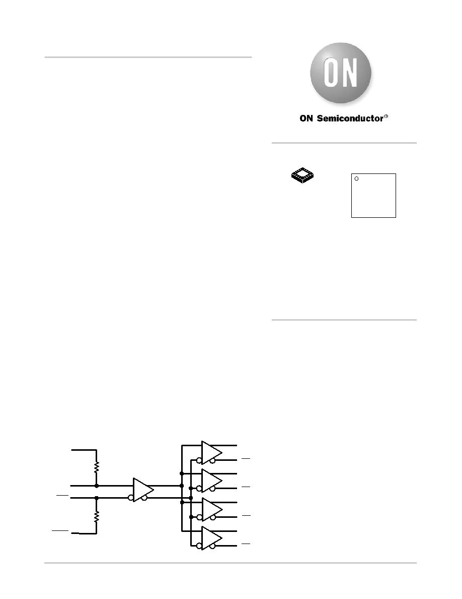
Figure 1. Logic Diagram
50 W
VTCLK
CLK
VTCLK
Q3
Q2
Q1
Q0
http://onsemi.com
*For additional marking information, refer to
Application Note AND8002/D.
MARKING
DIAGRAM*
A
= Assembly Location
L
= Wafer Lot
Y
= Year
W
= Work Week
G
= PbFree Package
QFN16
MN SUFFIX
CASE 485G
16
NB7L
14M
ALYWG
G
1
See detailed ordering and shipping information in the package
dimensions section on page 10 of this data sheet.
ORDERING INFORMATION
(Note: Microdot may be in either location)
1
相关PDF资料 |
PDF描述 |
|---|---|
| AD9743BCPZRL | IC DAC DUAL 10B 250MSPS 72-LFCSP |
| NB7L11MMN | IC CLK/DTA BUF TRNSLA 1:2 16-QFN |
| LTC2642ACMS-16#TRPBF | IC DAC 16BIT V-OUT 10-MSOP |
| LTC2642ACDD-16#TRPBF | IC DAC 16BIT VOUT 10-DFN |
| NB7L111MMN | IC CLK/DATA BUFF MUX 2:10 52-QFN |
相关代理商/技术参数 |
参数描述 |
|---|---|
| NB7L14MMNEVB | 功能描述:时钟和定时器开发工具 BBG NB7L14MMN EVAL BOARD RoHS:否 制造商:Texas Instruments 产品:Evaluation Modules 类型:Clock Conditioners 工具用于评估:LMK04100B 频率:122.8 MHz 工作电源电压:3.3 V |
| NB7L14MMNG | 功能描述:时钟缓冲器 2.5V/3.3V Multilevel 1:4 Clock / Fanout RoHS:否 制造商:Texas Instruments 输出端数量:5 最大输入频率:40 MHz 传播延迟(最大值): 电源电压-最大:3.45 V 电源电压-最小:2.375 V 最大功率耗散: 最大工作温度:+ 85 C 最小工作温度:- 40 C 封装 / 箱体:LLP-24 封装:Reel |
| NB7L14MMNR2 | 功能描述:时钟缓冲器 2.5V/3.3V Multilevel RoHS:否 制造商:Texas Instruments 输出端数量:5 最大输入频率:40 MHz 传播延迟(最大值): 电源电压-最大:3.45 V 电源电压-最小:2.375 V 最大功率耗散: 最大工作温度:+ 85 C 最小工作温度:- 40 C 封装 / 箱体:LLP-24 封装:Reel |
| NB7L14MMNR2G | 功能描述:时钟缓冲器 2.5V/3.3V Multilevel 1:4 Clock / Fanout RoHS:否 制造商:Texas Instruments 输出端数量:5 最大输入频率:40 MHz 传播延迟(最大值): 电源电压-最大:3.45 V 电源电压-最小:2.375 V 最大功率耗散: 最大工作温度:+ 85 C 最小工作温度:- 40 C 封装 / 箱体:LLP-24 封装:Reel |
| NB7L14MN1G | 功能描述:时钟缓冲器 2.5V/3.3V FANOUT BUFFER RoHS:否 制造商:Texas Instruments 输出端数量:5 最大输入频率:40 MHz 传播延迟(最大值): 电源电压-最大:3.45 V 电源电压-最小:2.375 V 最大功率耗散: 最大工作温度:+ 85 C 最小工作温度:- 40 C 封装 / 箱体:LLP-24 封装:Reel |
发布紧急采购,3分钟左右您将得到回复。