参数资料
| 型号: | NB7L14MMN |
| 厂商: | ON Semiconductor |
| 文件页数: | 4/11页 |
| 文件大小: | 0K |
| 描述: | IC CLK/DTA BUF TRNSLA 1:4 16-QFN |
| 产品变化通告: | LTB Notification 06/Feb/2008 |
| 标准包装: | 123 |
| 类型: | 扇出缓冲器(分配),变换器,数据 |
| 电路数: | 1 |
| 比率 - 输入:输出: | 1:4 |
| 差分 - 输入:输出: | 是/是 |
| 输入: | CML,LVCMOS,LVDS,LVPECL,LVTTL |
| 输出: | CML |
| 频率 - 最大: | 8GHz |
| 电源电压: | 2.375 V ~ 3.465 V |
| 工作温度: | -40°C ~ 85°C |
| 安装类型: | 表面贴装 |
| 封装/外壳: | 16-VFQFN 裸露焊盘 |
| 供应商设备封装: | 16-QFN(3x3) |
| 包装: | 管件 |
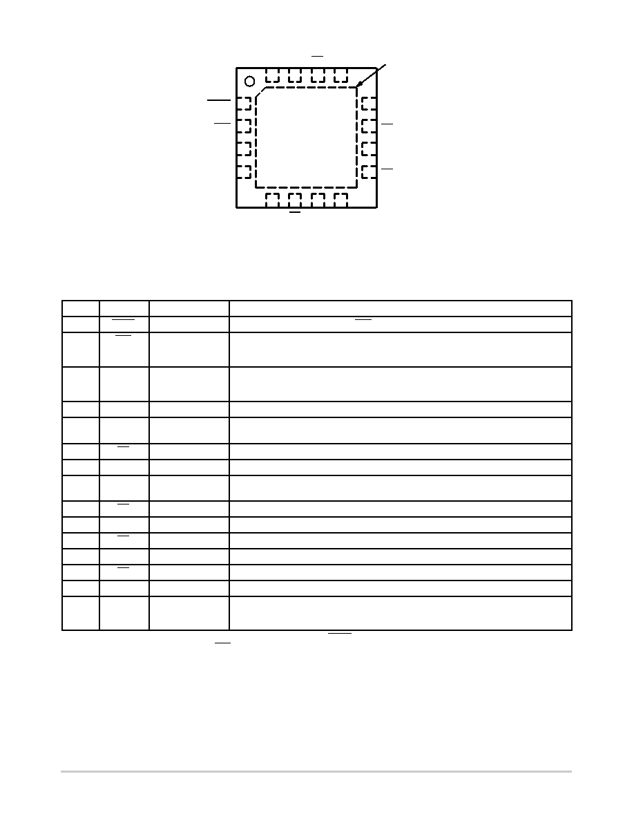
NB7L14M
http://onsemi.com
2
VEE Q3
Q3 VCC
VEE Q0
Q0
VCC
Q1
Q2
VTCLK
CLK
VTCLK
56
7
8
16
15
14
13
12
11
10
9
1
2
3
4
NB7L14M
Exposed Pad (EP)
Figure 2. QFN16 Pinout (Top View)
Table 1. PIN DESCRIPTION
Pin
Name
I/O
Description
1
VTCLK
Internal 50 W Termination Pin for CLK.
2
CLK
LVPECL, CML,
LVCMOS, LVTTL,
LVDS
Inverted Differential Clock/Data Input. (Note 1)
3
CLK
LVPECL, CML,
LVCMOS, LVTTL,
LVDS
Noninverted Differential Clock/Data Input. (Note 1)
4
VTCLK
Internal 50 W Termination Pin for CLK.
5,16
VEE
Power Supply
Negative Supply Voltage. All VEE pins must be externally connected to a Power Supply to
guarantee proper operation.
6
Q3
CML Output
Inverted Differential Output 3 with Internal 50 W Source Termination Resistor. (Note 2)
7
Q3
CML Output
Noninverted Differential Output 3 with Internal 50 W Source Termination Resistor. (Note 2)
8,13
VCC
Power Supply
Positive Supply Voltage. All VCC pins must be externally connected to a Power Supply to
guarantee proper operation.
9
Q2
CML Output
Inverted Differential Output 2 with Internal 50 W Source Termination Resistor. (Note 2)
10
Q2
CML Output
Noninverted Differential Output 2 with Internal 50 W Source Termination Resistor. (Note 2)
11
Q1
CML Output
Inverted Differential Output 1 with Internal 50 W Source Termination Resistor. (Note 2)
12
Q1
CML Output
Noninverted Differential Output 1 with Internal 50 W Source Termination Resistor. (Note 2)
14
Q0
CML Output
Inverted Differential Output 0 with Internal 50 W Source Termination Resistor. (Note 2)
15
Q0
CML Output
Noninverted Differential Output 0 with Internal 50 W Source Termination Resistor. (Note 2)
EP
Exposed Pad. Thermal pad on the package bottom must be attached to a heatsinking
conduit to improve heat transfer. It is recommended to connect the EP to the lower
potential (VEE).
1. In the differential configuration when the input termination pins (VTCLK, VTCLK) are connected to a common termination voltage or left open,
and if no signal is applied on CLK and CLK, then the device will be susceptible to selfoscillation.
2. CML outputs require 50 W receiver termination resistors to VCC for proper operation.
相关PDF资料 |
PDF描述 |
|---|---|
| AD9743BCPZRL | IC DAC DUAL 10B 250MSPS 72-LFCSP |
| NB7L11MMN | IC CLK/DTA BUF TRNSLA 1:2 16-QFN |
| LTC2642ACMS-16#TRPBF | IC DAC 16BIT V-OUT 10-MSOP |
| LTC2642ACDD-16#TRPBF | IC DAC 16BIT VOUT 10-DFN |
| NB7L111MMN | IC CLK/DATA BUFF MUX 2:10 52-QFN |
相关代理商/技术参数 |
参数描述 |
|---|---|
| NB7L14MMNEVB | 功能描述:时钟和定时器开发工具 BBG NB7L14MMN EVAL BOARD RoHS:否 制造商:Texas Instruments 产品:Evaluation Modules 类型:Clock Conditioners 工具用于评估:LMK04100B 频率:122.8 MHz 工作电源电压:3.3 V |
| NB7L14MMNG | 功能描述:时钟缓冲器 2.5V/3.3V Multilevel 1:4 Clock / Fanout RoHS:否 制造商:Texas Instruments 输出端数量:5 最大输入频率:40 MHz 传播延迟(最大值): 电源电压-最大:3.45 V 电源电压-最小:2.375 V 最大功率耗散: 最大工作温度:+ 85 C 最小工作温度:- 40 C 封装 / 箱体:LLP-24 封装:Reel |
| NB7L14MMNR2 | 功能描述:时钟缓冲器 2.5V/3.3V Multilevel RoHS:否 制造商:Texas Instruments 输出端数量:5 最大输入频率:40 MHz 传播延迟(最大值): 电源电压-最大:3.45 V 电源电压-最小:2.375 V 最大功率耗散: 最大工作温度:+ 85 C 最小工作温度:- 40 C 封装 / 箱体:LLP-24 封装:Reel |
| NB7L14MMNR2G | 功能描述:时钟缓冲器 2.5V/3.3V Multilevel 1:4 Clock / Fanout RoHS:否 制造商:Texas Instruments 输出端数量:5 最大输入频率:40 MHz 传播延迟(最大值): 电源电压-最大:3.45 V 电源电压-最小:2.375 V 最大功率耗散: 最大工作温度:+ 85 C 最小工作温度:- 40 C 封装 / 箱体:LLP-24 封装:Reel |
| NB7L14MN1G | 功能描述:时钟缓冲器 2.5V/3.3V FANOUT BUFFER RoHS:否 制造商:Texas Instruments 输出端数量:5 最大输入频率:40 MHz 传播延迟(最大值): 电源电压-最大:3.45 V 电源电压-最小:2.375 V 最大功率耗散: 最大工作温度:+ 85 C 最小工作温度:- 40 C 封装 / 箱体:LLP-24 封装:Reel |
发布紧急采购,3分钟左右您将得到回复。