参数资料
| 型号: | NB7L11MMN |
| 厂商: | ON Semiconductor |
| 文件页数: | 1/11页 |
| 文件大小: | 0K |
| 描述: | IC CLK/DTA BUF TRNSLA 1:2 16-QFN |
| 产品变化通告: | LTB Notification 06/Feb/2008 |
| 标准包装: | 123 |
| 类型: | 扇出缓冲器(分配),变换器,数据 |
| 电路数: | 1 |
| 比率 - 输入:输出: | 1:2 |
| 差分 - 输入:输出: | 是/是 |
| 输入: | CML,LVCMOS,LVDS,LVPECL,LVTTL |
| 输出: | CML |
| 频率 - 最大: | 8GHz |
| 电源电压: | 2.375 V ~ 3.465 V |
| 工作温度: | -40°C ~ 85°C |
| 安装类型: | 表面贴装 |
| 封装/外壳: | 16-VFQFN 裸露焊盘 |
| 供应商设备封装: | 16-QFN(3x3) |
| 包装: | 管件 |
Semiconductor Components Industries, LLC, 2011
January, 2011 Rev. 3
1
Publication Order Number:
NB7L11M/D
NB7L11M
2.5V/3.3V Differential 1:2
Clock/Data Fanout Buffer/
Translator with CML
Outputs and Internal
Termination
Description
The NB7L11M is a differential 1to2 clock/data distribution chip
with internal source termination and CML output structure, optimized
for low skew and minimal jitter. The device is functionally equivalent to
the EP11, LVEP11, or SG11 devices. Device produces two identical
output copies of clock or data operating up to 8 GHz or 12 Gb/s,
respectively. As such, NB7L11M is ideal for SONET, GigE, Fiber
Channel, Backplane and other clock/data distribution applications.
Inputs incorporate internal 50
W termination resistors and accept
LVPECL, CML, LVCMOS, LVTTL, or LVDS (See Table 6).
Differential 16 mA CML output provides matching internal 50
W
terminations, and 400 mV output swings when externally terminated,
50
The device is offered in a low profile 3x3 mm 16pin QFN package.
Application notes, models, and support documentation are available at
www.onsemi.com.
Features
Maximum Input Clock Frequency up to 8 GHz Typical
Maximum Input Data Rate up to 12 Gb/s Typical
< 0.5 ps of RMS Clock Jitter
< 10 ps of Data Dependent Jitter
30 ps Typical Rise and Fall Times
110 ps Typical Propagation Delay
3 ps Typical Within Device Skew
Operating Range: VCC = 2.375 V to 3.465 V with VEE = 0 V
CML Output Level (400 mV PeaktoPeak Output) Differential
Output Only
50 W Internal Input and Output Termination Resistors
Functionally Compatible with Existing 2.5 V/3.3 V LVEL, LVEP, EP
and SG Devices
PbFree Packages are Available
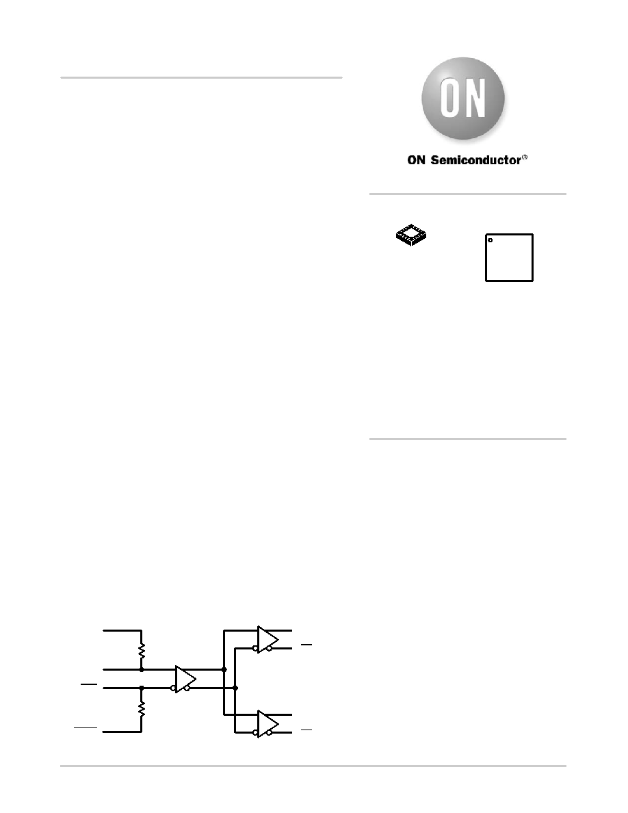
Figure 1. Logic Diagram
Q0
Q1
VTCLK
CLK
VTCLK
50 W
*For additional marking information, refer to
Application Note AND8002/D.
MARKING
DIAGRAM*
A
= Assembly Location
L
= Wafer Lot
Y
= Year
W
= Work Week
G
= PbFree Package
QFN16
MN SUFFIX
CASE 485G
http://onsemi.com
See detailed ordering and shipping information in the package
dimensions section on page 10 of this data sheet.
ORDERING INFORMATION
(Note: Microdot may be in either location)
NB7L
11M
ALYWG
G
1
相关PDF资料 |
PDF描述 |
|---|---|
| LTC2642ACMS-16#TRPBF | IC DAC 16BIT V-OUT 10-MSOP |
| LTC2642ACDD-16#TRPBF | IC DAC 16BIT VOUT 10-DFN |
| NB7L111MMN | IC CLK/DATA BUFF MUX 2:10 52-QFN |
| LTC2641ACMS8-16#TRPBF | IC DAC 16BIT VOUT 8-MSOP |
| LTC2641ACDD-16#TRPBF | IC DAC 16BIT VOUT 8-DFN |
相关代理商/技术参数 |
参数描述 |
|---|---|
| NB7L11MMNEVB | 功能描述:BOARD EVAL BBG NB7L11MMN RoHS:是 类别:编程器,开发系统 >> 评估演示板和套件 系列:* 标准包装:1 系列:PCI Express® (PCIe) 主要目的:接口,收发器,PCI Express 嵌入式:- 已用 IC / 零件:DS80PCI800 主要属性:- 次要属性:- 已供物品:板 |
| NB7L11MMNG | 功能描述:时钟缓冲器 2.5V/3.3V Multilevel 1:2 Clock / Fanout RoHS:否 制造商:Texas Instruments 输出端数量:5 最大输入频率:40 MHz 传播延迟(最大值): 电源电压-最大:3.45 V 电源电压-最小:2.375 V 最大功率耗散: 最大工作温度:+ 85 C 最小工作温度:- 40 C 封装 / 箱体:LLP-24 封装:Reel |
| NB7L11MMNR2 | 功能描述:时钟缓冲器 2.5V/3.3V Multilevel RoHS:否 制造商:Texas Instruments 输出端数量:5 最大输入频率:40 MHz 传播延迟(最大值): 电源电压-最大:3.45 V 电源电压-最小:2.375 V 最大功率耗散: 最大工作温度:+ 85 C 最小工作温度:- 40 C 封装 / 箱体:LLP-24 封装:Reel |
| NB7L11MMNR2G | 功能描述:时钟缓冲器 2.5V/3.3V Multilevel 1:2 Clock / Fanout RoHS:否 制造商:Texas Instruments 输出端数量:5 最大输入频率:40 MHz 传播延迟(最大值): 电源电压-最大:3.45 V 电源电压-最小:2.375 V 最大功率耗散: 最大工作温度:+ 85 C 最小工作温度:- 40 C 封装 / 箱体:LLP-24 封装:Reel |
| NB7L14 | 制造商:ONSEMI 制造商全称:ON Semiconductor 功能描述:2.5V / 3.3V 7GHz/10Gbps Differential 1:4 LVPECL Fanout Buffer |
发布紧急采购,3分钟左右您将得到回复。