参数资料
| 型号: | NB7L11MMN |
| 厂商: | ON Semiconductor |
| 文件页数: | 6/11页 |
| 文件大小: | 0K |
| 描述: | IC CLK/DTA BUF TRNSLA 1:2 16-QFN |
| 产品变化通告: | LTB Notification 06/Feb/2008 |
| 标准包装: | 123 |
| 类型: | 扇出缓冲器(分配),变换器,数据 |
| 电路数: | 1 |
| 比率 - 输入:输出: | 1:2 |
| 差分 - 输入:输出: | 是/是 |
| 输入: | CML,LVCMOS,LVDS,LVPECL,LVTTL |
| 输出: | CML |
| 频率 - 最大: | 8GHz |
| 电源电压: | 2.375 V ~ 3.465 V |
| 工作温度: | -40°C ~ 85°C |
| 安装类型: | 表面贴装 |
| 封装/外壳: | 16-VFQFN 裸露焊盘 |
| 供应商设备封装: | 16-QFN(3x3) |
| 包装: | 管件 |
NB7L11M
http://onsemi.com
4
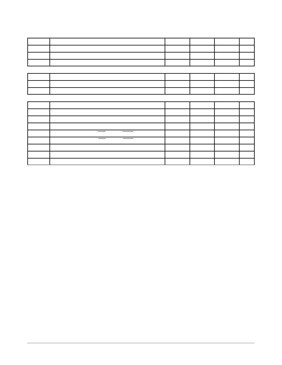
Table 4. DC CHARACTERISTICS, CLOCK Inputs, CML Outputs (VCC = 2.375 V to 3.465 V, VEE = 0 V, TA = 40°C to +85°C)
(Note 5)
Symbol
Characteristic
Min
Typ
Max
Unit
ICC
Power Supply Current (Input and Outputs open)
85
105
mA
VOH
Output HIGH Voltage (Note 6)
VCC 60
VCC 20
VCC
mV
VOL
Output LOW Voltage (Note 6)
VCC 530
VCC 420
VCC 360
mV
Vth
Input Threshold Reference Voltage Range (Note 7)
1125
VCC 75
mV
VIH
Singleended Input HIGH Voltage (Note 8)
Vth + 75
VCC
mV
VIL
Singleended Input LOW Voltage (Note 8)
VEE
Vth 75
mV
VIHCLK
Differential Input HIGH Voltage
1200
VCC
mV
VILCLK
Differential Input LOW Voltage
VEE
VCC 75
mV
VCMR
Input Common Mode Range (Differential Configuration)
1163
VCC – 38
mV
VID
Differential Input Voltage (VIHCLK VILCLK)
75
2500
mV
IIH
Input HIGH Current
CLK / CLK
(VTCLK/VTCLK Open)
0
25
100
mA
IIL
Input LOW Current
CLK / CLK
(VTCLK/VTCLK Open)
10
0
10
mA
RTIN
Internal Input Termination Resistor
45
50
55
W
RTOUT
Internal Output Termination Resistor
45
50
55
W
RTemp Coef Internal I/O Termination Resistor Temperature Coefficient
6.38
mW/°C
NOTE: Device will meet the specifications after thermal equilibrium has been established when mounted in a test socket or printed circuit
board with maintained transverse airflow greater than 500 lfpm. Electrical parameters are guaranteed only over the declared
operating temperature range. Functional operation of the device exceeding these conditions is not implied. Device specification limit
values are applied individually under normal operating conditions and not valid simultaneously.
5. Input and output parameters vary 1:1 with VCC.
6. CML outputs require 50 W receiver termination resistors to VCC for proper operation.
7. Vth is applied to the complementary input when operating in singleended mode.
8. VCMR min varies 1:1 with VEE, VCMR max varies 1:1 with VCC.
相关PDF资料 |
PDF描述 |
|---|---|
| LTC2642ACMS-16#TRPBF | IC DAC 16BIT V-OUT 10-MSOP |
| LTC2642ACDD-16#TRPBF | IC DAC 16BIT VOUT 10-DFN |
| NB7L111MMN | IC CLK/DATA BUFF MUX 2:10 52-QFN |
| LTC2641ACMS8-16#TRPBF | IC DAC 16BIT VOUT 8-MSOP |
| LTC2641ACDD-16#TRPBF | IC DAC 16BIT VOUT 8-DFN |
相关代理商/技术参数 |
参数描述 |
|---|---|
| NB7L11MMNEVB | 功能描述:BOARD EVAL BBG NB7L11MMN RoHS:是 类别:编程器,开发系统 >> 评估演示板和套件 系列:* 标准包装:1 系列:PCI Express® (PCIe) 主要目的:接口,收发器,PCI Express 嵌入式:- 已用 IC / 零件:DS80PCI800 主要属性:- 次要属性:- 已供物品:板 |
| NB7L11MMNG | 功能描述:时钟缓冲器 2.5V/3.3V Multilevel 1:2 Clock / Fanout RoHS:否 制造商:Texas Instruments 输出端数量:5 最大输入频率:40 MHz 传播延迟(最大值): 电源电压-最大:3.45 V 电源电压-最小:2.375 V 最大功率耗散: 最大工作温度:+ 85 C 最小工作温度:- 40 C 封装 / 箱体:LLP-24 封装:Reel |
| NB7L11MMNR2 | 功能描述:时钟缓冲器 2.5V/3.3V Multilevel RoHS:否 制造商:Texas Instruments 输出端数量:5 最大输入频率:40 MHz 传播延迟(最大值): 电源电压-最大:3.45 V 电源电压-最小:2.375 V 最大功率耗散: 最大工作温度:+ 85 C 最小工作温度:- 40 C 封装 / 箱体:LLP-24 封装:Reel |
| NB7L11MMNR2G | 功能描述:时钟缓冲器 2.5V/3.3V Multilevel 1:2 Clock / Fanout RoHS:否 制造商:Texas Instruments 输出端数量:5 最大输入频率:40 MHz 传播延迟(最大值): 电源电压-最大:3.45 V 电源电压-最小:2.375 V 最大功率耗散: 最大工作温度:+ 85 C 最小工作温度:- 40 C 封装 / 箱体:LLP-24 封装:Reel |
| NB7L14 | 制造商:ONSEMI 制造商全称:ON Semiconductor 功能描述:2.5V / 3.3V 7GHz/10Gbps Differential 1:4 LVPECL Fanout Buffer |
发布紧急采购,3分钟左右您将得到回复。