参数资料
| 型号: | NB7L11MMN |
| 厂商: | ON Semiconductor |
| 文件页数: | 4/11页 |
| 文件大小: | 0K |
| 描述: | IC CLK/DTA BUF TRNSLA 1:2 16-QFN |
| 产品变化通告: | LTB Notification 06/Feb/2008 |
| 标准包装: | 123 |
| 类型: | 扇出缓冲器(分配),变换器,数据 |
| 电路数: | 1 |
| 比率 - 输入:输出: | 1:2 |
| 差分 - 输入:输出: | 是/是 |
| 输入: | CML,LVCMOS,LVDS,LVPECL,LVTTL |
| 输出: | CML |
| 频率 - 最大: | 8GHz |
| 电源电压: | 2.375 V ~ 3.465 V |
| 工作温度: | -40°C ~ 85°C |
| 安装类型: | 表面贴装 |
| 封装/外壳: | 16-VFQFN 裸露焊盘 |
| 供应商设备封装: | 16-QFN(3x3) |
| 包装: | 管件 |
NB7L11M
http://onsemi.com
2
VCC Q1 Q1
VCC
VCC Q0
Q0
VCC
VEE
VTCLK
CLK
VTCLK
56
7
8
16
15
14
13
12
11
10
9
1
2
3
4
NB7L11M
Exposed Pad (EP)
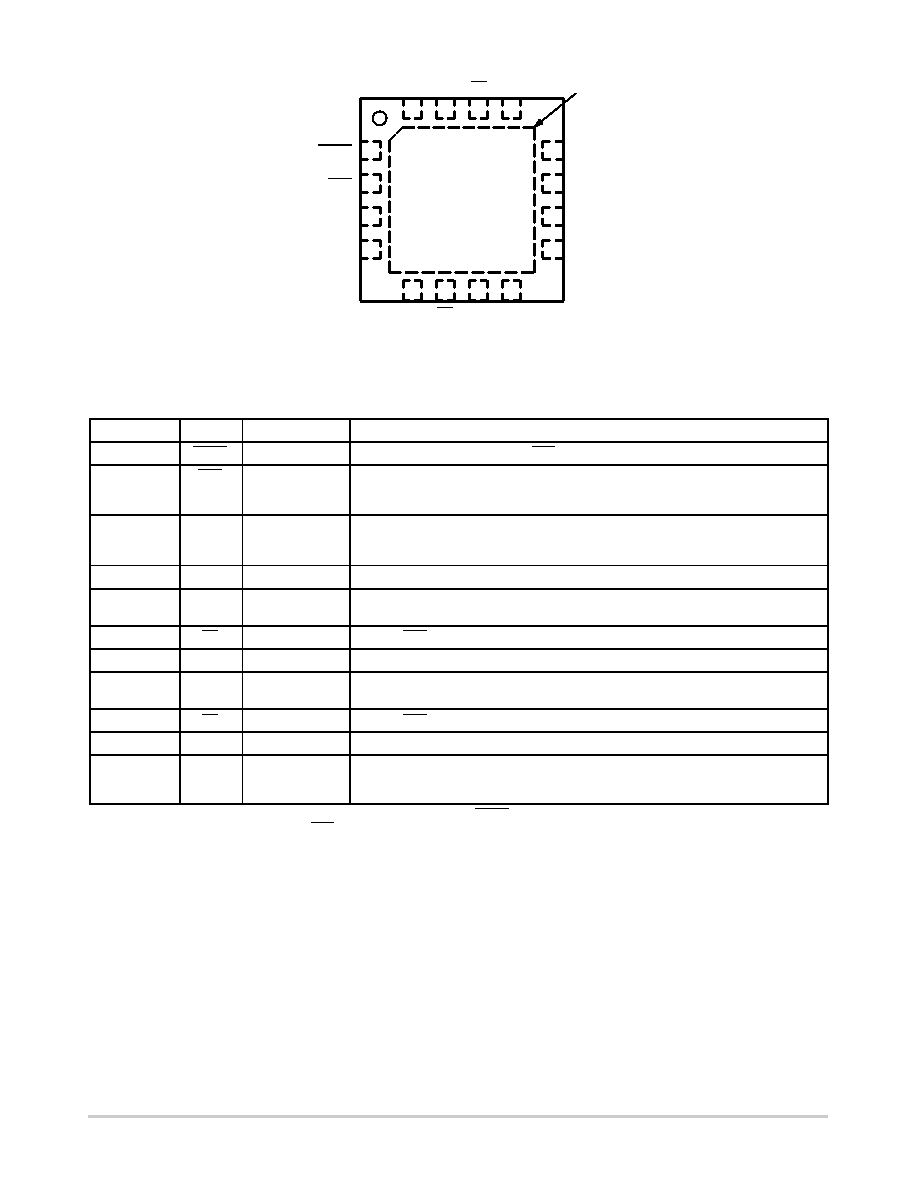
Figure 2. QFN16 Pinout (Top View)
Table 1. PIN DESCRIPTION
Pin
Name
I/O
Description
1
VTCLK
Internal 50 W Termination Pin for CLK
2
CLK
LVPECL, CML,
LVCMOS, LVTTL,
LVDS
Inverted Differential Clock/Data Input. (Note 1)
3
CLK
LVPECL, CML,
LVCMOS, LVTTL,
LVDS
Noninverted Differential Clock/Data Input. (Note 1)
4
VTCLK
Internal 50 W Termination Pin for CLK
5,8,13,16
VCC
Positive Supply Voltage. All VCC pins must be externally connected to a Power Supply
to guarantee proper operation.
6
Q1
CML Output
Inverted CLK output 1 with internal 50 W source termination resistor. (Note 2)
7
Q1
CML Output
Noninverted CLK output 1 with internal 50 W source termination resistor. (Note 2)
9,10,11,12
VEE
Negative Supply Voltage. All VEE pins must be externally connected to a Power Supply
to guarantee proper operation.
14
Q0
CML Output
Inverted CLK output 0 with internal 50 W source termination resistor. (Note 2)
15
Q0
CML Output
Noninverted CLK output 0 with internal 50 W source termination resistor. (Note 2)
EP
Exposed Pad. The thermally exposed pad on package bottom (see case drawing) must
be attached to a heatsinking conduit. It is recommended to connect the EP to the lower
potential (VEE).
1. In the differential configuration when the input termination pins (VTCLK, VTCLK) are connected to a common termination voltage or left open,
and if no signal is applied on CLK and CLK then the device will be susceptible to selfoscillation.
2. CML outputs require 50 W receiver termination resistor to VCC for proper operation.
相关PDF资料 |
PDF描述 |
|---|---|
| LTC2642ACMS-16#TRPBF | IC DAC 16BIT V-OUT 10-MSOP |
| LTC2642ACDD-16#TRPBF | IC DAC 16BIT VOUT 10-DFN |
| NB7L111MMN | IC CLK/DATA BUFF MUX 2:10 52-QFN |
| LTC2641ACMS8-16#TRPBF | IC DAC 16BIT VOUT 8-MSOP |
| LTC2641ACDD-16#TRPBF | IC DAC 16BIT VOUT 8-DFN |
相关代理商/技术参数 |
参数描述 |
|---|---|
| NB7L11MMNEVB | 功能描述:BOARD EVAL BBG NB7L11MMN RoHS:是 类别:编程器,开发系统 >> 评估演示板和套件 系列:* 标准包装:1 系列:PCI Express® (PCIe) 主要目的:接口,收发器,PCI Express 嵌入式:- 已用 IC / 零件:DS80PCI800 主要属性:- 次要属性:- 已供物品:板 |
| NB7L11MMNG | 功能描述:时钟缓冲器 2.5V/3.3V Multilevel 1:2 Clock / Fanout RoHS:否 制造商:Texas Instruments 输出端数量:5 最大输入频率:40 MHz 传播延迟(最大值): 电源电压-最大:3.45 V 电源电压-最小:2.375 V 最大功率耗散: 最大工作温度:+ 85 C 最小工作温度:- 40 C 封装 / 箱体:LLP-24 封装:Reel |
| NB7L11MMNR2 | 功能描述:时钟缓冲器 2.5V/3.3V Multilevel RoHS:否 制造商:Texas Instruments 输出端数量:5 最大输入频率:40 MHz 传播延迟(最大值): 电源电压-最大:3.45 V 电源电压-最小:2.375 V 最大功率耗散: 最大工作温度:+ 85 C 最小工作温度:- 40 C 封装 / 箱体:LLP-24 封装:Reel |
| NB7L11MMNR2G | 功能描述:时钟缓冲器 2.5V/3.3V Multilevel 1:2 Clock / Fanout RoHS:否 制造商:Texas Instruments 输出端数量:5 最大输入频率:40 MHz 传播延迟(最大值): 电源电压-最大:3.45 V 电源电压-最小:2.375 V 最大功率耗散: 最大工作温度:+ 85 C 最小工作温度:- 40 C 封装 / 箱体:LLP-24 封装:Reel |
| NB7L14 | 制造商:ONSEMI 制造商全称:ON Semiconductor 功能描述:2.5V / 3.3V 7GHz/10Gbps Differential 1:4 LVPECL Fanout Buffer |
发布紧急采购,3分钟左右您将得到回复。