参数资料
| 型号: | NB4L6254FAG |
| 厂商: | ON Semiconductor |
| 文件页数: | 1/11页 |
| 文件大小: | 0K |
| 描述: | IC CLK MUX SWITCH 1:6/1:3 32LQFP |
| 标准包装: | 250 |
| 类型: | 多路复用器,开关 |
| 电路数: | 1 或 2 |
| 比率 - 输入:输出: | 1:6,1:3 |
| 差分 - 输入:输出: | 是/是 |
| 输入: | LVCMOS,LVPECL |
| 输出: | LVPECL |
| 频率 - 最大: | 3GHz |
| 电源电压: | 2.375 V ~ 3.465 V |
| 工作温度: | -40°C ~ 85°C |
| 安装类型: | 表面贴装 |
| 封装/外壳: | 32-LQFP |
| 供应商设备封装: | 32-LQFP(7x7) |
| 包装: | 托盘 |
Semiconductor Components Industries, LLC, 2009
March, 2009 Rev. 3
1
Publication Order Number:
NB4L6254/D
NB4L6254
2.5V / 3.3V Differential
LVPECL 2x2 Clock Switch
and Low Skew Fanout
Buffer
Description
The NB4L6254 is a differential 2x2 clock switch and drives
precisely aligned clock signals through its LVPECL fanout buffers. It
employs a fully differential architecture with bipolar technology,
offers superior digital signal characteristics, has very low clock output
skew and supports clock frequencies from DC up to 3.0 GHz.
The NB4L6254 is designed for the most demanding, skew critical
differential clock distribution systems. Typical applications for the
NB4L6254 are clock distribution, switching and data loopback
systems of highperformance computer, networking and
telecommunication systems, as well as onboard clocking of OC3,
OC12 and OC48 communication systems. In addition, the
NB4L6254 can be configured as a single 1:6 or dual 1:3 LVPECL
fanout buffer.
The NB4L6254 can be operated from a single 3.3 V or 2.5 V power
supply.
Features
Maximum Clock Input Frequency, 3 GHz
Maximum Input Data Rate, 3 Gb/s
Differential LVPECL Inputs and Outputs
Low Output Skew: 50 ps Maximum OutputtoOutput Skew
Synchronous Output Enable Eliminating Output Runt Pulse
Generation and Metastability
Operating Range: Single 3.3 V or 2.5 V Supply
VCC = 2.375 V to 3.465 V
LVCMOS Compatible Control Inputs
Packaged in LQFP32
Fully Differential Architecture
40°C to 85°C Ambient Operating Temperature
These are PbFree Devices*
*For additional information on our PbFree strategy and soldering details, please
download the ON Semiconductor Soldering and Mounting Techniques
Reference Manual, SOLDERRM/D.
LQFP32
FA SUFFIX
CASE 873A
MARKING DIAGRAMS*
http://onsemi.com
*For additional marking information, refer to
Application Note AND8002/D.
See detailed ordering and shipping information in the package
dimensions section on page 9 of this data sheet.
ORDERING INFORMATION
A
= Assembly Location
WL
= Wafer Lot
YY
= Year
WW
= Work Week
G or G = PbFree Package
(Note: Microdot may be in either location)
NB4L
6254
AWLYYWWG
32
1
NB4L6254
AWLYYWWG
G
1
QFN32
MN SUFFIX
CASE 488AM
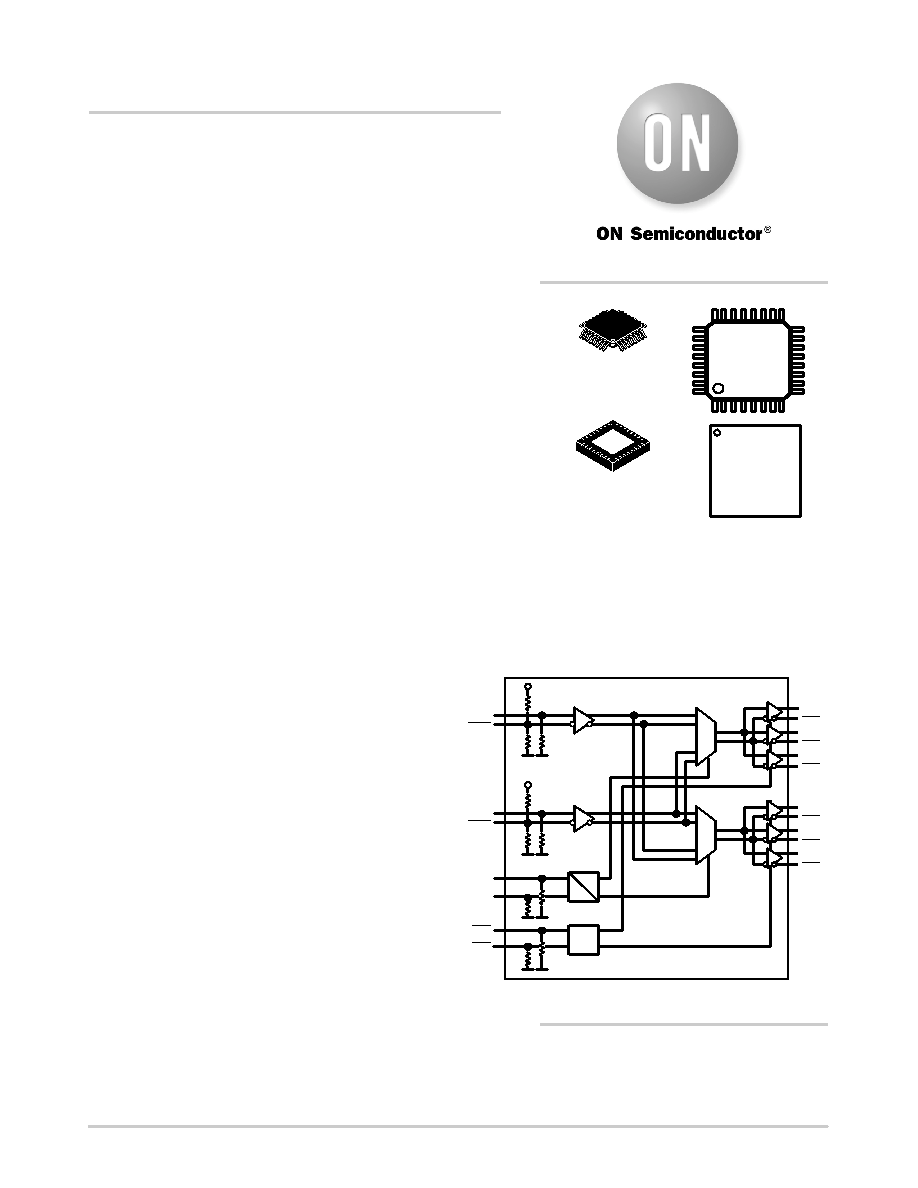
OEA
QA0
QA1
QA2
QB0
QB1
QB2
0
1
0
1
Bank A
Bank B
OEB
SEL0
SEL1
CLK1
CLK0
VCC
Figure 1. Functional Block Diagram
SYNC
相关PDF资料 |
PDF描述 |
|---|---|
| V300A12H500BG3 | CONVERTER MOD DC/DC 12V 500W |
| V300A12H500BG | CONVERTER MOD DC/DC 12V 500W |
| AD5323BRUZ-REEL7 | IC DAC 12BIT DUAL R-R 16-TSSOP |
| V300A12H500BF2 | CONVERTER MOD DC/DC 12V 500W |
| V300A12H500BF | CONVERTER MOD DC/DC 12V 500W |
相关代理商/技术参数 |
参数描述 |
|---|---|
| NB4L6254FAR2G | 功能描述:模拟和数字交叉点 IC AIT LVPECL 2X2 SW FN RoHS:否 制造商:Micrel 配置:2 x 2 封装 / 箱体:MLF-16 数据速率:10.7 Gbps 输入电平:CML, LVDS, LVPECL 输出电平:CML 电源电压-最大:3.6 V 电源电压-最小:2.375 V 最大工作温度:+ 85 C 最小工作温度:- 40 C 产品:Digital Crosspoint 封装:Tube |
| NB4L6254MNG | 功能描述:时钟驱动器及分配 LVPECL 2X2 SWITCH FANOUT RoHS:否 制造商:Micrel 乘法/除法因子:1:4 输出类型:Differential 最大输出频率:4.2 GHz 电源电压-最大: 电源电压-最小:5 V 最大工作温度:+ 85 C 封装 / 箱体:SOIC-8 封装:Reel |
| NB4L6254MNR4G | 功能描述:时钟驱动器及分配 LVPECL 2X2 SWITCH FANOUT RoHS:否 制造商:Micrel 乘法/除法因子:1:4 输出类型:Differential 最大输出频率:4.2 GHz 电源电压-最大: 电源电压-最小:5 V 最大工作温度:+ 85 C 封装 / 箱体:SOIC-8 封装:Reel |
| NB4L7210 | 制造商:ONSEMI 制造商全称:ON Semiconductor 功能描述:2.5V/3.3V Differential 2x10 Crosspoint Clock Driver with SDI Programmable Output Selects |
| NB4L7210MNG | 功能描述:时钟驱动器及分配 DIFF HSTL ECL PECL CLK RoHS:否 制造商:Micrel 乘法/除法因子:1:4 输出类型:Differential 最大输出频率:4.2 GHz 电源电压-最大: 电源电压-最小:5 V 最大工作温度:+ 85 C 封装 / 箱体:SOIC-8 封装:Reel |
发布紧急采购,3分钟左右您将得到回复。