- 您现在的位置:买卖IC网 > PDF目录11168 > NB4L858MFAR2G (ON Semiconductor)IC CROSSPOINT SWITCH DUAL 32LQFP PDF资料下载
参数资料
| 型号: | NB4L858MFAR2G |
| 厂商: | ON Semiconductor |
| 文件页数: | 4/10页 |
| 文件大小: | 0K |
| 描述: | IC CROSSPOINT SWITCH DUAL 32LQFP |
| 标准包装: | 2,000 |
| 功能: | 交叉点开关 |
| 电路: | 2 x 2:2 |
| 电压电源: | 单电源 |
| 电压 - 电源,单路/双路(±): | 2.3 V ~ 3.6 V |
| 电流 - 电源: | 130mA |
| 工作温度: | -40°C ~ 85°C |
| 安装类型: | 表面贴装 |
| 封装/外壳: | 32-LQFP |
| 供应商设备封装: | 32-LQFP(7x7) |
| 包装: | 带卷 (TR) |
NB4L858M
http://onsemi.com
3
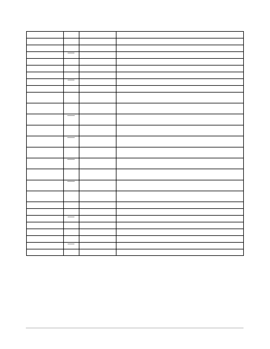
Table 2. PIN DESCRIPTION
Pin
Name
I/O
Description
1
DB1
LVPECL, CML Input
Channel B1 positive signal input.
2
VTDB1
Internal 100
W centertapped termination pin for channel B1.
3
DB1
LVPECL, CML Input
Channel B1 negative signal input.
4
SELB0
LVTTL / LVCMOS
Channel B0 Output Select. See Table 1.
5
DB0
LVPECL, CML Input
Channel B0 positive signal input.
6
VTDB0
Internal 100
W centertapped termination pin for channel B0.
7
DB0
LVPECL, CML Input
Channel B0 negative signal input.
8
SELB1
LVTTL / LVCMOS
Channel B1 output select. See Table 1.
9,24
GND
Supply ground. All GND pins must be externally connected to power supply to
guarantee proper operation.
10, 13, 16, 17, 20, 23
VCC
Positive Supply. All VCC pins must be externally connected to power supply to
guarantee proper operation.
11
QB0
CML Output
Channel B0 negative signal output. Typically terminated with 50
W resistor to
VCC.
12
QB0
CML Output
Channel B0 positive signal output. Typically terminated with 50
W resistor to
VCC
14
QB1
CML Output
Channel B1 negative signal output. Typically terminated with 50
W resistor to
VCC.
15
QB1
CML Output
Channel B1 positive signal output. Typically terminated with 50
W resistor to
VCC.
18
QA1
CML Output
Channel A1 negative signal output. Typically terminated with 50
W resistor to
VCC.
19
QA1
CML Output
Channel A1 positive signal output. Typically terminated with 50
W resistor to
VCC.
21
QA0
CML Output
Channel A0 negative signal output. Typically terminated with 50
W resistor to
VCC.
22
QA0
CML Output
Channel A0 positive signal output. Typically terminated with 50
W resistor to
VCC.
25
DA0
LVPECL, CML Input
Channel A0 positive signal input.
26
VTDA0
Internal 100
W centertapped termination pin for channel A0.
27
DA0
LVPECL, CML Input
Channel A0 negative signal input.
28
SELA1
LVTTL
Channel A1 output select. See Table 1.
29
DA1
LVPECL, CML Input
Channel A1 positive signal input.
30
VTDA1
Internal 100
W centertapped termination pin for channel A1.
31
DA1
LVPECL, CML Input
Channel A1 negative signal input.
32
SELA0
LVTTL
Channel A0 output select. See Table 1.
相关PDF资料 |
PDF描述 |
|---|---|
| HI1-0509-2 | IC MULTIPLEXER DUAL 4X1 16CDIP |
| EFM32TG210F8 | MCU 32BIT 8KB FLASH 32-QFN |
| HI9P5051-9Z | IC SWITCH DUAL SPDT 16SOIC |
| NB7V72MMNHTBG | IC CROSSPOINT SWITCH 2X2 16-QFN |
| VE-B1X-CU-B1 | CONVERTER MOD DC/DC 5.2V 200W |
相关代理商/技术参数 |
参数描述 |
|---|---|
| NB4MAAH0-0-B | 制造商:未知厂家 制造商全称:未知厂家 功能描述:N e u t r i k ?? P a r t N u m b e r G u i d e |
| NB4MAH0-0-B | 制造商:未知厂家 制造商全称:未知厂家 功能描述:N e u t r i k ?? P a r t N u m b e r G u i d e |
| NB4N111K | 制造商:ONSEMI 制造商全称:ON Semiconductor 功能描述:3.3V Differential In 1:10 Differential Fanout Clock Driver with HCSL Level Output |
| NB4N111KMNG | 功能描述:时钟缓冲器 TSMC 1:10 FANOUT BUF HCSL RoHS:否 制造商:Texas Instruments 输出端数量:5 最大输入频率:40 MHz 传播延迟(最大值): 电源电压-最大:3.45 V 电源电压-最小:2.375 V 最大功率耗散: 最大工作温度:+ 85 C 最小工作温度:- 40 C 封装 / 箱体:LLP-24 封装:Reel |
| NB4N111KMNR4G | 功能描述:时钟缓冲器 TSMC 1:10 FANOUT BUF HCSL RoHS:否 制造商:Texas Instruments 输出端数量:5 最大输入频率:40 MHz 传播延迟(最大值): 电源电压-最大:3.45 V 电源电压-最小:2.375 V 最大功率耗散: 最大工作温度:+ 85 C 最小工作温度:- 40 C 封装 / 箱体:LLP-24 封装:Reel |
发布紧急采购,3分钟左右您将得到回复。