- 您现在的位置:买卖IC网 > PDF目录11168 > NB4L858MFAR2G (ON Semiconductor)IC CROSSPOINT SWITCH DUAL 32LQFP PDF资料下载
参数资料
| 型号: | NB4L858MFAR2G |
| 厂商: | ON Semiconductor |
| 文件页数: | 7/10页 |
| 文件大小: | 0K |
| 描述: | IC CROSSPOINT SWITCH DUAL 32LQFP |
| 标准包装: | 2,000 |
| 功能: | 交叉点开关 |
| 电路: | 2 x 2:2 |
| 电压电源: | 单电源 |
| 电压 - 电源,单路/双路(±): | 2.3 V ~ 3.6 V |
| 电流 - 电源: | 130mA |
| 工作温度: | -40°C ~ 85°C |
| 安装类型: | 表面贴装 |
| 封装/外壳: | 32-LQFP |
| 供应商设备封装: | 32-LQFP(7x7) |
| 包装: | 带卷 (TR) |
NB4L858M
http://onsemi.com
6
Symbol
Characteristic
40
°C
25
°C
85
°C
Unit
Min
Typ
Max
Min
Typ
Max
Min
Typ
Max
VOUTPP
Output Voltage Amplitude (@ VINPPmin)
fin ≤ 2 GHz
(See Figure 2)
fin ≤ 3 GHz
fin ≤ 3.5GHz
280
235
170
365
310
220
280
235
170
365
310
220
280
235
170
365
310
220
mV
fDATA
Maximum Operating Data Rate
3
Gb/s
tPLH,
tPHL
Propagation Delay to Output Differential
D/D to Q/Q
220
350
450
220
350
450
220
350
450
ps
tSWiITCH
SELyx to Valid Qyx Output (Note 9)
0.5
1.0
0.5
1.0
0.5
1.0
ns
tSKEW
Within Device Skew (Note 5)
Within Device Skew (Note 6)
Device to Device Skew (Note 9)
12
25
100
12
25
100
12
25
100
ps
tJITTER
RMS Random Clock Jitter (Note 8)
fin =2 GHz
fin =3 GHz
PeaktoPeak Data Dependent Jitter fin =2.5Gb/s
(Note 9)
fin =3.2Gb/s
Crosstalk Induced RMS Jitter (Note 11)
0.5
1.0
2.0
10
0.5
1.0
5.0
10
0.5
1.0
2.0
10
0.5
ps
VINPP
Input Voltage Swing/Sensitivity
(Differential Configuration)
100
800
100
800
100
800
mV
tr
tf
Output Rise/Fall Times @ 0.5 GHz
Qx, Qx
(20% 80%)
80
120
80
120
80
120
ps
NOTE: Device will meet the specifications after thermal equilibrium has been established when mounted in a test socket or printed circuit
board with maintained transverse airflow greater than 500 lfpm. Electrical parameters are guaranteed only over the declared
operating temperature range. Functional operation of the device exceeding these conditions is not implied. Device specification limit
values are applied individually under normal operating conditions and not valid simultaneously.
4. Measured by forcing VINPP (MIN) from a 50% duty cycle clock source. All loading with an external RL = 50 W to VCC. Input edge rates 40 ps
(20% 80%).
5. Worstcase difference between QA0 and QA1 from either DA0 or DA1 (or between QB0 and QB1 from either DB0 or DB1 respectively),
when both outputs come from the same input.
6. Worstcase difference between QA and QB outputs, when DA or DB inputs are shorted.
7. Additive RMS jitter with 50% duty cycle input clock signal.
8. Additive peaktopeak data dependent jitter with input NRZ data signal.
9. Device to device skew is measured between outputs under identical transition @ 0.5 GHz.
10. LVTTL/LVCMOS input edge rate less than 1.5 ns
11. Data taken on the same device under identical condition.
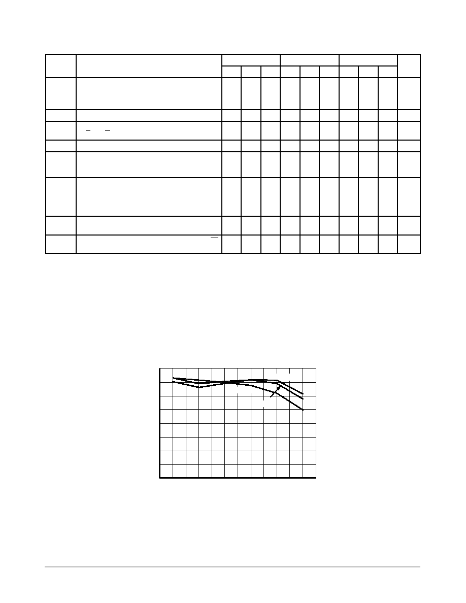
Figure 2. Output Voltage Amplitude (VOUTPP) versus Input Clock Frequency (fin) and Temperature
0
50
100
150
200
250
300
350
400
1
1.5
2
2.5
3
3.5
VOL
T
AGE
(mV)
INPUT CLOCK FREQUENCY (GHz)
25
°C
40
°C
85
°C
相关PDF资料 |
PDF描述 |
|---|---|
| HI1-0509-2 | IC MULTIPLEXER DUAL 4X1 16CDIP |
| EFM32TG210F8 | MCU 32BIT 8KB FLASH 32-QFN |
| HI9P5051-9Z | IC SWITCH DUAL SPDT 16SOIC |
| NB7V72MMNHTBG | IC CROSSPOINT SWITCH 2X2 16-QFN |
| VE-B1X-CU-B1 | CONVERTER MOD DC/DC 5.2V 200W |
相关代理商/技术参数 |
参数描述 |
|---|---|
| NB4MAAH0-0-B | 制造商:未知厂家 制造商全称:未知厂家 功能描述:N e u t r i k ?? P a r t N u m b e r G u i d e |
| NB4MAH0-0-B | 制造商:未知厂家 制造商全称:未知厂家 功能描述:N e u t r i k ?? P a r t N u m b e r G u i d e |
| NB4N111K | 制造商:ONSEMI 制造商全称:ON Semiconductor 功能描述:3.3V Differential In 1:10 Differential Fanout Clock Driver with HCSL Level Output |
| NB4N111KMNG | 功能描述:时钟缓冲器 TSMC 1:10 FANOUT BUF HCSL RoHS:否 制造商:Texas Instruments 输出端数量:5 最大输入频率:40 MHz 传播延迟(最大值): 电源电压-最大:3.45 V 电源电压-最小:2.375 V 最大功率耗散: 最大工作温度:+ 85 C 最小工作温度:- 40 C 封装 / 箱体:LLP-24 封装:Reel |
| NB4N111KMNR4G | 功能描述:时钟缓冲器 TSMC 1:10 FANOUT BUF HCSL RoHS:否 制造商:Texas Instruments 输出端数量:5 最大输入频率:40 MHz 传播延迟(最大值): 电源电压-最大:3.45 V 电源电压-最小:2.375 V 最大功率耗散: 最大工作温度:+ 85 C 最小工作温度:- 40 C 封装 / 箱体:LLP-24 封装:Reel |
发布紧急采购,3分钟左右您将得到回复。